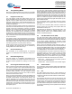
Distributed by: www.Jameco.com ✦ 1-800-831-4242 The content and copyrights of the attached material are the property of its owner.
CY7C63722C CY7C63723C CY7C63743C enCoRe™ USB Combination Low-Speed USB and PS/2 Peripheral Controller 1.0 Features • enCoRe™ USB - enhanced Component Reduction — Internal oscillator eliminates the need for an external crystal or resonator — Interface can auto-configure to operate as PS/2 or USB without the need for external components to switch between modes (no General Purpose I/O [GPIO] pins needed to manage dual mode capability) — Internal 3.
CY7C63722C CY7C63723C CY7C63743C FOR FOR 2.0 Logic Block Diagram XTALIN/P2.1 XTALOUT Internal Oscillator Xtal Oscillator EPROM 8K Byte 8-bit RISC Core Brown-out Reset Watch Dog Timer Low Voltage Reset 3.0 3.1 Wake-Up Timer RAM 256 Byte 12-bit Timer Capture Timers Interrupt Controller USB Engine Port 1 GPIO Port 0 GPIO 3.3V Regulator USB & PS/2 Xcvr VREG/P2.
CY7C63722C CY7C63723C CY7C63743C FOR FOR The USB D+ and D– USB pins can alternately be used as PS/2 SCLK and SDATA signals, so that products can be designed to respond to either USB or PS/2 modes of operation. PS/2 operation is supported with internal pull-up resistors on SCLK and SDATA, the ability to disable the regulator output pin, and an interrupt to signal the start of PS/2 activity.
CY7C63722C CY7C63723C CY7C63743C FOR FOR 6.0 Programming Model Refer to the CYASM Assembler User’s Guide for more details on firmware operation with the CY7C637xxC microcontrollers. 6.1 Program Counter (PC) The 14-bit program counter (PC) allows access for up to 8 Kbytes of EPROM using the CY7C637xxC architecture. The program counter is cleared during reset, such that the first instruction executed after a reset is at address 0x0000.
CY7C63722C CY7C63723C CY7C63743C FOR FOR 6.6.3 • DSPINIT: EQU 30h • MOV A,DSPINIT 6.6.2 Direct “Direct” address mode is used when the data operand is a variable stored in SRAM. In that case, the one byte address of the variable is encoded in the instruction.
CY7C63722C CY7C63723C CY7C63743C FOR FOR MNEMONIC Operand Opcode MNEMONIC Cycles Operand Opcode Cycles MOV A,[expr] direct 1A 5 CPL 3A 4 MOV A,[X+expr] index 1B 6 ASL 3B 4 MOV X,expr data 1C 4 ASR 3C 4 MOV X,[expr] direct 1D 5 RLC 3D 4 reserved 1E RRC 3E 4 XPAGE 1F 4 RET 3F 8 MOV A,X 40 4 DI 70 4 MOV X,A 41 4 EI 72 4 MOV PSP,A 60 4 RETI 73 8 50 - 5F 10 CALL addr JMP addr 80-8F 5 JC addr C0-CF 5 (or 4) CALL addr 90-9F 10 JNC
CY7C63722C CY7C63723C CY7C63743C FOR FOR 8.0 8.1 Memory Organization Program Memory Organization[1] After reset 14 -bit PC Address 0x0000 Program execution begins here after a reset 0x0002 USB Bus Reset interrupt vector 0x0004 128-µs timer interrupt vector 0x0006 1.
CY7C63722C CY7C63723C CY7C63743C FOR FOR 8.2 Data Memory Organization The CY7C637xxC microcontrollers provide 256 bytes of data RAM. In normal usage, the SRAM is partitioned into four areas: program stack, data stack, user variables and USB endpoint FIFOs as shown below.
CY7C63722C CY7C63723C CY7C63743C FOR FOR Table 8-1. I/O Register Summary (continued) Register Name I/O Address Read/Write Function Fig.
CY7C63722C CY7C63723C CY7C63743C FOR FOR 9.0 Clocking The chip can be clocked from either the internal on-chip clock, or from an oscillator based on an external resonator/crystal, as shown in Figure 9-1. No additional capacitance is included on chip at the XTALIN/OUT pins. Operation is controlled by the Clock Configuration Register, Figure 9-2. Int Clk Output Disable XTALOUT Internal Osc Ext Clk Enable Clock Doubler Clk2x (12 MHz) (to Microcontroller) XTALIN Clk1x (6 MHz) (to USB SIE) Port 2.
CY7C63722C CY7C63723C CY7C63743C FOR FOR mov A, 1h before the part executes code. See Section 10.1 for more details. 1 = Disables the LVR circuit. iowr F8h 0 = Enables the LVR circuit. Bit 2: Precision USB Clocking Enable The Precision USB Clocking Enable only affects operation in internal oscillator mode. In that mode, this bit must be set to 1 to cause the internal clock to automatically precisely tune to USB timing requirements (6 MHz ±1.5%).
CY7C63722C CY7C63723C CY7C63743C FOR FOR The microcontroller begins execution from ROM address 0x0000 after a LVR, BOR, or WDR reset. Although this looks like interrupt vector 0, there is an important difference. Reset processing does NOT push the program counter, carry flag, and zero flag onto program stack. Attempting to execute either a RET or RETI in the reset handler will cause unpredictable execution results. The following events take place on reset.
CY7C63722C CY7C63723C CY7C63743C FOR FOR 11.0 Suspend Mode The CY7C637xxC parts support a versatile low-power suspend mode. In suspend mode, only an enabled interrupt or a LOW state on the D–/SDATA pin will wake the part. Two options are available. For lowest power, all internal circuits can be disabled, so only an external event will resume operation. Alternatively, a low-power internal wake-up timer can be used to trigger the wake-up interrupt. This timer is described in Section 11.
CY7C63722C CY7C63723C CY7C63743C FOR FOR Table 11-1. Wake-up Timer Adjust Settings Adjust Bits [2:0] (Bits [6:4] in Figure 9-2) Wake-up Time 000 (reset state) 1 * tWAKE 001 2 * tWAKE 010 4 * tWAKE 011 8 * tWAKE 100 16 * tWAKE 101 32 * tWAKE 110 64 * tWAKE 111 128 * tWAKE See Section 26.0 for the value of tWAKE 12.0 General Purpose I/O Ports Ports 0 and 1 provide up to 16 versatile GPIO pins that can be read or written (the number of pins depends on package type).
CY7C63722C CY7C63723C CY7C63743C FOR FOR Bit # 7 6 5 4 Bit Name 3 2 1 0 P0 Read/Write R/W R/W R/W R/W R/W R/W R/W R/W Reset 0 0 0 0 0 0 0 0 Figure 12-2. Port 0 Data (Address 0x00) 1 = Port Pin is logic HIGH 0 = Port Pin is logic LOW 7 6 5 4 3 2 1 0 P1 Pins 7:2 only in CY7C63743C Pins 1:0 in all parts Read/Write R/W R/W R/W R/W R/W R/W R/W R/W Reset 0 0 0 0 0 0 0 0 2 1 0 Figure 12-3.
CY7C63722C CY7C63723C CY7C63743C FOR FOR 13.0 Table 12-1. Ports 0 and 1 Output Control Truth Table Data Register Mode1 Mode0 Output Drive Input Strength Threshold 0 1 0 0 0 0 1 1 0 1 0 1 0 1 1 1 12.1 Hi-Z CMOS Hi-Z TTL Medium (8 mA) Sink CMOS High Drive CMOS Low (2 mA) Sink CMOS Resistive CMOS High (50 mA) Sink CMOS High Drive CMOS Auxiliary Input Port Port 2 serves as an auxiliary input port as shown in Figure 12-8. The Port 2 inputs all have TTL input thresholds.
CY7C63722C CY7C63723C CY7C63743C FOR FOR 13.2 USB Port Status and Control USB status and control is regulated by the USB Status and Control Register as shown in Figure 13-1. Bit # 7 6 5 4 3 2:0 Bit PS/2 VREG USB Reserved USB D+/D– Name Pull-up Enable ResetBus Forcing Activity Bit Enable PS/2 Activity Interrupt Mode Read/ R/W Write Reset 0 R/W R/W - R/W R/W 0 0 0 0 0 0 0 Figure 13-1.
CY7C63722C CY7C63723C CY7C63743C FOR FOR 14.0 USB Device The CY7C637xxC supports one USB Device Address with three endpoints: EP0, EP1, and EP2. 14.1 USB Address Register The USB Device Address Register contains a 7-bit USB address and one bit to enable USB communication. This register is cleared during a reset, setting the USB device address to zero and marking this address as disabled. Figure 14-1 shows the format of the USB Address Register.
CY7C63722C CY7C63723C CY7C63743C FOR FOR In addition, the Mode Bits are automatically changed by the SIE in response to many USB transactions. For example, if the Mode Bit [3:0] are set to 1011 which is ACK OUT-NAK IN mode as shown in Table 22-1, the SIE will change the endpoint Mode Bit [3:0] to NAK IN/OUT (0001) mode after issuing an ACK handshake in response to an OUT token. Firmware needs to update the mode for the SIE to respond appropriately. 14.
CY7C63722C CY7C63723C CY7C63743C FOR FOR 15.0 USB Regulator Output The VREG pin provides a regulated output for connecting the pull-up resistor required for USB operation. For USB, a 1.5-kΩ resistor is connected between the D– pin and the VREG voltage, to indicate low-speed USB operation. Since the VREG output has an internal series resistance of approximately 200Ω, the external pull-up resistor required is RPU (see Section 25.0).
CY7C63722C CY7C63723C CY7C63743C FOR FOR 17.0 Serial Peripheral Interface (SPI) SPI is a four-wire, full-duplex serial communication interface between a master device and one or more slave devices. The CY7C637xxC SPI circuit supports byte serial transfers in either Master or Slave modes. The block diagram of the SPI circuit is shown in Figure 17-1. The block contains buffers for Data Bus both transmit and receive data for maximum flexibility and throughput.
CY7C63722C CY7C63723C CY7C63743C FOR FOR hardware provides 8 output clocks on the SCK pin (P0.7) for each byte transfer. Clock phase and polarity are selected by the CPHA and CPOL control bits (see Figure 17-1 and 17-4). The master SCK duty cycle is nominally 33% in the fastest (2 Mbps) mode, and 50% in all other modes. 17.3 Operation as an SPI Slave In slave mode, the chip receives SCK from an external master on pin P0.7. Data from the master is shifted in on the MOSI pin (P0.
CY7C63722C CY7C63723C CY7C63743C FOR FOR SCK (CPOL = 0) SCK (CPOL = 1) SS CPHA = 0: MOSI/MISO x MSB LSB Data Capture Strobe Interrupt Issued CPHA = 1: MOSI/MISO MSB LSB x Data Capture Strobe Interrupt Issued Figure 17-4. SPI Data Timing 17.5 SPI Interrupt For SPI, an interrupt request is generated after a byte is received or transmitted. See Section 21.3 for details on the SPI interrupt. 17.6 SPI Modes for GPIO Pins The GPIO pins used for SPI outputs (P0.5–P0.
CY7C63722C CY7C63723C CY7C63743C FOR FOR 18.0 12-bit Free-running Timer Bit [7:0]: Timer lower eight bits The 12-bit timer operates with a 1-µs tick, provides two interrupts (128-µs and 1.024-ms) and allows the firmware to directly time events that are up to 4 ms in duration. The lower eight bits of the timer can be read directly by the firmware. Reading the lower eight bits latches the upper four bits into a temporary register.
CY7C63722C CY7C63723C CY7C63743C FOR FOR 19.0 Timer Capture Registers capture eight bits of the free-running timer into its Capture Timer Data Register if a rising or falling edge event that matches the specified rising or falling edge condition at the pin. A prescaler allows selection of the capture timer tick size. Interrupts can be individually enabled for the four capture registers. A block diagram is shown in Figure 19-1.
CY7C63722C CY7C63723C CY7C63743C FOR FOR Bit # 7 6 Read/Write R R R R R Reset 0 0 0 0 0 Bit Name 5 4 3 2 1 0 R R R 0 0 0 Capture A Falling Data Figure 19-3. Capture Timer A-Falling, Data Register (Address 0x41) Bit # 7 6 Bit Name 5 4 3 2 1 0 Capture B Rising Data Read/Write R R R R R R R R Reset 0 0 0 0 0 0 0 0 Figure 19-4.
CY7C63722C CY7C63723C CY7C63743C FOR FOR 20.0 Processor Status and Control Register Bit # 7 6 5 4 3 2 1 0 Bit Name IRQ Pending Watchdog Reset Bus Interrupt Event LVR/BOR Reset Suspend Interrupt Enable Sense Reserved Run Read/Write R R/W R/W R/W R/W R - R/W Reset 0 1 0 1 0 0 0 1 Figure 20-1. Processor Status and Control Register (Address 0xFF) Bit 7: IRQ Pending When an interrupt is generated, it is registered as a pending interrupt.
CY7C63722C CY7C63723C CY7C63743C FOR FOR During a Watchdog Reset, the Processor Status and Control Register is set to 01XX0001, which indicates a Watchdog Reset (bit 4 set) has occurred and no interrupts are pending (bit 7 clear). 21.0 Interrupts Interrupts can be generated by the GPIO lines, the internal free-running timer, the SPI block, the capture timers, on various USB events, PS/2 activity, or by the wake-up timer.
CY7C63722C CY7C63723C CY7C63743C FOR FOR 21.3 Interrupt Sources The following sections provide details on the different types of interrupt sources. Bit # 7 6 5 4 3 2 1 0 Bit Name Wake-up Interrupt Enable GPIO Interrupt Enable Capture Timer B Intr. Enable Capture Timer A Intr. Enable SPI Interrupt Enable 1.024-ms Interrupt Enable 128-µs Interrupt Enable USB Bus Reset / PS/2 Activity Intr.
CY7C63722C CY7C63723C CY7C63743C FOR FOR A USB bus reset is indicated by a single ended zero (SE0) on the USB D+ and D– pins. The USB Bus Reset interrupt occurs when the SE0 condition ends. PS/2 activity is indicated by a continuous LOW on the SDATA pin. The PS/2 interrupt occurs as soon as the long LOW state is detected. During the entire interval of a USB Bus Reset or PS/2 interrupt event, the USB Device Address register is cleared.
CY7C63722C CY7C63723C CY7C63743C FOR FOR USB-PS/2 Clear Interrupt Vector CLR 1 Q D USBPS/2 Int CLK USB-PS/2 IRQ 128-µs CLR 128-µs IRQ 1-ms CLR 1-ms IRQ Enable [0] (Reg 0x20) CPU CLR Q D EP2 Int CLK (Bit 7, Reg 0xFF) IRQ EP1 CLR EP1 IRQ EP2 CLR EP2 IRQ Enable [2] (Reg 0x21) IRQ Pending IRQout EP0 CLR EP0 IRQ 1 To CPU Global Interrupt Enable Bit SPI CLR SPI IRQ Capture A CLR Capture A IRQ (Bit 2, Reg 0xFF) Controlled by DI, EI, and RETI Instructions CLR Capture B CLR Capture B IRQ
CY7C63722C CY7C63723C CY7C63743C FOR FOR Bit [7:0]: P1[7:0] Interrupt Polarity 1 = Rising GPIO edge 0 = Falling GPIO edge Port Bit Interrupt Polarity Register OR Gate (1 input per GPIO pin) M U X GPIO Pin 1 = Enable 0 = Disable GPIO Interrupt Flip Flop 1 D Q CLR Interrupt Priority Encoder IRQout Interrupt Vector Port Bit Interrupt Enable Register IRA 1 = Enable 0 = Disable Global GPIO Interrupt Enable (Bit 6, Register 0x20) Figure 21-8. GPIO Interrupt Diagram 22.
CY7C63722C CY7C63723C CY7C63743C FOR FOR Mode Column: [3:0] of the Endpoint Count Register (Figure 14-4) in response to any IN token. The 'Mode' column contains the mnemonic names given to the modes of the endpoint. The mode of the endpoint is determined by the four-bit binaries in the 'Encoding' column as discussed below. The Status IN and Status OUT modes represent the status IN or OUT stage of the control transfer.
CY7C63722C CY7C63723C CY7C63743C FOR FOR The response of the SIE can be summarized as follows: 1. The SIE will only respond to valid transactions, and will ignore non-valid ones. 2. The SIE will generate an interrupt when a valid transaction is completed or when the FIFO is corrupted. FIFO corruption occurs during an OUT or SETUP transaction to a valid internal address, that ends with a non-valid CRC. 3.
CY7C63722C CY7C63723C CY7C63743C FOR FOR Table 22-3.
CY7C63722C CY7C63723C CY7C63743C FOR FOR Table 22-3. Details of Modes for Differing Traffic Conditions (continued) 1 1 0 0 OUT x UC x UC UC UC UC UC UC UC NoChange Ignore no 1 1 0 0 IN x UC x UC UC UC UC 1 UC UC NoChange NAK yes Reserved 0 1 1 1 Out x UC x UC UC UC UC UC UC UC NoChange Ignore no 0 1 1 1 IN x UC x UC UC UC UC 1 UC UC NoChange TX yes Document #: 38-08022 Rev.
CY7C63722C CY7C63723C CY7C63743C FOR FOR 23.0 Register Summary Register Name Bit 6 Bit 5 INTERRUPT TIMER SPI CAPTURE TIMER PROC SC.
CY7C63722C CY7C63723C CY7C63743C FOR FOR 24.0 Absolute Maximum Ratings Storage Temperature ..........................................................................................................................................–65°C to +150°C Ambient Temperature with Power Applied ...............................................................................................................–0°C to +70°C Supply Voltage on VCC Relative to VSS ............................................................
CY7C63722C CY7C63723C CY7C63743C FOR FOR 25.0 DC Characteristics FOSC = 6 MHz; Operating Temperature = 0 to 70°C (continued) Parameter Conditions Min. Max. Unit VOLU Static Output Low With RPU to VREG pin VOHZ Static Output High, idle or suspend RPD connected D– to Gnd, RPU connected D– to VREG pin[4] 2.7 0.3 V 3.6 V VDI Differential Input Sensitivity |(D+)–(D–)| 0.2 VCM Differential Input Common Mode Range 0.8 2.5 V VSE Single Ended Receiver Threshold 0.8 2.
CY7C63722C CY7C63723C CY7C63743C FOR FOR 26.0 Switching Characteristics Parameter Description Conditions Min. Max. Unit Internal Clock Mode FICLK Internal Clock Frequency Internal Clock Mode enabled 5.7 6.3 MHz FICLK2 Internal Clock Frequency, USB mode Internal Clock Mode enabled, Bit 2 of register 0xF8h is set (Precision USB Clocking)[12] 5.91 6.09 MHz TCYC Input Clock Cycle Time USB Operation, with External ±1.5% Ceramic Resonator or Crystal 164.2 169.
CY7C63722C CY7C63723C CY7C63743C FOR FOR 26.0 Switching Characteristics (continued) Parameter Description Conditions Min. Max.
CY7C63722C CY7C63723C CY7C63743C FOR FOR TPERIOD Differential Data Lines TJR TJR1 TJR2 Consecutive Transitions N * TPERIOD + TJR1 Paired Transitions N * TPERIOD + TJR2 Figure 26-3. Receiver Jitter Tolerance TPERIOD Crossover Point Extended Crossover Point Differential Data Lines Diff. Data to SE0 Skew N * TPERIOD + TDEOP Source EOP Width: TEOPT Receiver EOP Width: TEOPR1, TEOPR2 Figure 26-4.
CY7C63722C CY7C63723C CY7C63743C FOR FOR SS (SS is under firmware control in SPI Master mode) TSCKL SCK (CPOL=0) TSCKH SCK (CPOL=1) TMDO MOSI MSB MSB MISO LSB LSB TMSU TMHD Figure 26-6. SPI Master Timing, CPHA = 0 SS TSSS TSSH TSCKL SCK (CPOL=0) TSCKH SCK (CPOL=1) MOSI MSB TSDO MISO LSB TSSU TSHD MSB LSB Figure 26-7. SPI Slave Timing, CPHA = 0 Document #: 38-08022 Rev.
CY7C63722C CY7C63723C CY7C63743C FOR FOR SS (SS is under firmware control in SPI Master mode) TSCKL SCK (CPOL=0) TSCKH SCK (CPOL=1) TMDO TMDO1 MOSI MSB LSB MSB MISO LSB TMSU TMHD Figure 26-8. SPI Master Timing, CPHA = 1 SS TSSH TSSS TSCKL SCK (CPOL=0) TSCKH SCK (CPOL=1) MSB MOSI LSB TSSU TSHD TSDO1 MISO TSDO MSB LSB Figure 26-9. SPI Slave Timing, CPHA = 1 Document #: 38-08022 Rev.
CY7C63722C CY7C63723C CY7C63743C FOR FOR 27.
CY7C63722C CY7C63723C CY7C63743C FOR FOR 28.0 Package Diagrams (continued) 24-Lead (300-Mil) SOIC S13 PIN 1 ID 12 1 DIMENSIONS IN INCHES[MM] * 0.394[10.007] 0.419[10.642] REFERENCE JEDEC MO-119 0.291[7.391] 0.300[7.620] 13 24 MIN. MAX. PACKAGE WEIGHT 0.65gms PART # S24.3 STANDARD PKG. SZ24.3 LEAD FREE PKG. 0.026[0.660] 0.032[0.812] SEATING PLANE 0.597[15.163] 0.615[15.621] 0.092[2.336] 0.105[2.667] * 0.050[1.270] TYP. 0.013[0.330] 0.019[0.482] * 0.004[0.101] 0.015[0.381] 0.050[1.270] 0.
CY7C63722C CY7C63723C CY7C63743C FOR FOR 28.0 Package Diagrams (continued) 24-Lead Quarter Size Outline Q13 51-85055-B DIE FORM Cypress Logo (1907, 3001) 3 2 1 25 24 23 Die Step: 1907 x 3011 microns Die Size: 1830.8 x 2909 microns Die Thickness: 14 mils = 355.6 microns Pad Size: 80 x 80 microns 10 17 (0,0) 13 14 15 16 22 21 20 19 18 11 12 Y 4 5 6 7 8 9 X Document #: 38-08022 Rev.
CY7C63722C CY7C63723C CY7C63743C Table 28-1 below shows the die pad coordinates for the CY7C63722C-XC. The center location of each bond pad is relative to the bottom left corner of the die which has coordinate (0,0). Table 28-1. CY7C63722C-XC Probe Pad Coordinates in microns ((0,0) to bond pad centers) Pad Number Pin Name X (microns) Y (microns) 1 P0.0 788.95 2843.15 2 P0.1 597.45 2843.15 3 P0.2 406.00 2843.15 4 P0.3 154.95 2687.95 5 P1.0 154.95 2496.45 6 P1.2 154.95 2305.
CY7C63722C CY7C63723C CY7C63743C FOR FOR Document History Page Document Title: CY7C63722C, CY7C63723C, CY7C63743C enCoRe™ USB Combination Low-Speed USB and PS/2 Peripheral Controller Document Number: 38-08022 REV. ECN NO. Issue Date Orig. of Change ** 118643 10/22/02 BON Converted from Spec 38-00944 to Spec 38-08022.