
User`s guide

CY7C63722C
CY7C63723C
CY7C63743C
FOR
FOR
Document #: 38-08022 Rev. *C Page 15 of 49
Bit [7:0]: P0[7:0]
1 = Port Pin is logic HIGH
0 = Port Pin is logic LOW
Bit [7:0]: P1[7:0]
1 = Port Pin is logic HIGH
0 = Port Pin is logic LOW
Bit [7:0]: P0[7:0] Mode 0
1 = Port 0 Mode 0 is logic HIGH
0 = Port 0 Mode 0 is logic LOW
Bit [7:0]: P0[7:0] Mode 1
1 = Port Pin Mode 1 is logic HIGH
0 = Port Pin Mode 1 is logic LOW
Bit [7:0]: P1[7:0] Mode 0
1 = Port Pin Mode 0 is logic HIGH
0 = Port Pin Mode 0 is logic LOW
Bit [7:0]: P1[7:0] Mode 1
1 = Port Pin Mode 1 is logic HIGH
0 = Port Pin Mode 1 is logic LOW
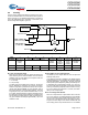
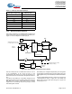
Each pin can be independently configured as high-impedance
inputs, inputs with internal pull-ups, open drain outputs, or
traditional CMOS outputs with selectable drive strengths.
The driving state of each GPIO pin is determined by the value
written to the pin’s Data Register and by its associated Mode0
and Mode1 bits. Table 12-1 lists the configuration states
based on these bits. The GPIO ports default on reset to all
Data and Mode Registers cleared, so the pins are all in a
high-impedance state. The available GPIO output drive
strength are:
• Hi-Z Mode (Mode1 = 0 and Mode0 = 0)
Q1, Q2, and Q3 (Figure 12-1) are OFF. The GPIO pin is not
driven internally. Performing a read from the Port Data Reg-
ister return the actual logic value on the port pins.
• Low Sink Mode (Mode1 = 1, Mode0 = 0, and the pin’s Data
Register = 0)
Q1 and Q3 are OFF. Q2 is ON. The GPIO pin is capable of
sinking 2 mA of current.
• Medium Sink Mode (Mode1 = 0, Mode0 = 1, and the pin’s
Data Register = 0)
Q1 and Q3 are OFF. Q2 is ON. The GPIO pin is capable of
sinking 8 mA of current.
• High Sink Mode (Mode1 = 1, Mode0 = 1, and the pin’s Data
Register = 0)
Q1 and Q3 are OFF. Q2 is ON. The GPIO pin is capable of
sinking 50 mA of current.
• High Drive Mode (Mode1 = 0 or 1, Mode0 = 1, and the pin’s
Data Register = 1)
Q1 and Q2 are OFF. Q3 is ON. The GPIO pin is capable of
sourcing 2 mA of current.
• Resistive Mode (Mode1 = 1, Mode0 = 0, and the pin’s Data
Register = 1)
Q2 and Q3 are OFF. Q1 is ON. The GPIO pin is pulled up
with an internal 14-kΩ resistor.
Note that open drain mode can be achieved by fixing the Data
and Mode1 Registers LOW, and switching the Mode0 register.
Input thresholds are CMOS, or TTL as shown in the table (See
Section 25.0 for the input threshold voltage in TTL or CMOS
modes). Both input modes include hysteresis to minimize
noise sensitivity. In suspend mode, if a pin is used for a
wake-up interrupt using an external R-C circuit, CMOS mode
is preferred for lowest power.
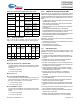
Bit # 76543210
Bit Name P0
Read/Write R/W R/W R/W R/W R/W R/W R/W R/W
Reset 00000000
Figure 12-2. Port 0 Data (Address 0x00)
Bit # 76543210
Bit Name P1
Notes Pins 7:2 only in CY7C63743C Pins 1:0 in
all parts
Read/Write R/W R/W R/W R/W R/W R/W R/W R/W
Reset 00000000
Figure 12-3. Port 1 Data (Address 0x01)
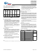
Bit # 76543210
Bit Name P0[7:0] Mode0
Read/Write WWWWWWWW
Reset 00000000
Figure 12-4. GPIO Port 0 Mode0 Register (Address 0x0A)
Bit # 76543210
Bit Name P0[7:0] Mode1
Read/Write WWWWWWWW
Reset 00000000
Figure 12-5. GPIO Port 0 Mode1 Register (Address 0x0B)
Bit # 76543210
Bit Name P1[7:0] Mode0
Read/Write WWWWWWWW
Reset 00000000
Figure 12-6. GPIO Port 1 Mode0 Register (Address 0x0C)
Bit # 76543210
Bit Name P1[7:0] Mode1
Read/Write WWWWWWWW
Reset 00000000
Figure 12-7. GPIO Port 1 Mode1 Register (Address 0x0D)