
User`s guide

CY7C63722C
CY7C63723C
CY7C63743C
FOR
FOR
Document #: 38-08022 Rev. *C Page 18 of 49
14.0 USB Device
The CY7C637xxC supports one USB Device Address with
three endpoints: EP0, EP1, and EP2.
14.1 USB Address Register
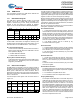
The USB Device Address Register contains a 7-bit USB
address and one bit to enable USB communication. This
register is cleared during a reset, setting the USB device
address to zero and marking this address as disabled.
Figure 14-1 shows the format of the USB Address Register.
In either USB or PS/2 mode, this register is cleared by both
hardware resets and the USB bus reset. See Section 21.3 for
more information on the USB Bus Reset – PS/2 interrupt.
Bit 7: Device Address Enable
This bit must be enabled by firmware before the serial in-
terface engine (SIE) will respond to USB traffic at the ad-
dress specified in Bit [6:0].
1 = Enable USB device address.
0 = Disable USB device address.
Bit [6:0]: Device Address Bit [6:0]
These bits must be set by firmware during the USB enumer-
ation process (i.e., SetAddress) to the non-zero address
assigned by the USB host.
14.2 USB Control Endpoint
All USB devices are required to have an endpoint number 0
(EP0) that is used to initialize and control the USB device. EP0
provides access to the device configuration information and
allows generic USB status and control accesses. EP0 is
bidirectional as the device can both receive and transmit data.
EP0 uses an 8-byte FIFO at SRAM locations 0xF8-0xFF, as
shown in Section 8.2.
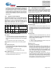
The EP0 endpoint mode register uses the format shown in
Figure 14-2.
The SIE provides a locking feature to prevent firmware from
overwriting bits in the USB Endpoint 0 Mode Register. Writes
to the register have no effect from the point that Bit[6:0] of the
register are updated (by the SIE) until the firmware reads this
register. The CPU can unlock this register by reading it.
Because of these hardware-locking features, firmware should
perform an read after a write to the USB Endpoint 0 Mode
Register and USB Endpoint 0 Count Register (Figure 14-4) to
verify that the contents have changed as desired, and that the
SIE has not updated these values.
Bit [7:4] of this register are cleared by any non-locked write to
this register, regardless of the value written.
Bit 7: SETUP Received
1 = A valid SETUP packet has been received. This bit is
forced HIGH from the start of the data packet phase of the
SETUP transaction until the start of the ACK packet re-
turned by the SIE. The CPU is prevented from clearing this
bit during this interval. While this bit is set to ‘1’, the CPU
cannot write to the EP0 FIFO. This prevents firmware from
overwriting an incoming SETUP transaction before firm-
ware has a chance to read the SETUP data.
0 = No SETUP received. This bit is cleared by any
non-locked writes to the register.
Bit 6: IN Received
1 = A valid IN packet has been received. This bit is updated
to ‘1’ after the last received packet in an IN transaction. This
bit is cleared by any non-locked writes to the register.
0 = No IN received. This bit is cleared by any non-locked
writes to the register.
Bit 5: OUT Received
1 = A valid OUT packet has been received. This bit is up-
dated to ‘1’ after the last received packet in an OUT trans-
action. This bit is cleared by any non-locked writes to the
register.
0 = No OUT received. This bit is cleared by any non-locked
writes to the register.
Bit 4: ACKed Transaction
The ACKed Transaction bit is set whenever the SIE engag-
es in a transaction to the register's endpoint that completes
with an ACK packet.
1 = The transaction completes with an ACK.
0 = The transaction does not complete with an ACK.
Bit [3:0]: Mode Bit[3:0]
The endpoint modes determine how the SIE responds to
USB traffic that the host sends to the endpoint. For exam-
ple, if the endpoint Mode Bits [3:0] are set to 0001 which is
NAK IN/OUT mode as shown in Table 22-1, the SIE will
send NAK handshakes in response to any IN or OUT token
sent to this endpoint. In this NAK IN/OUT mode, the SIE will
send an ACK handshake when the host sends a SETUP
token to this endpoint. The mode encoding is shown in
Table 22-1. Additional information on the mode bits can be
found in Table 22-2 and Table 22-3. These modes give the
firmware total control on how to respond to different tokens
sent to the endpoints from the host.
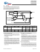
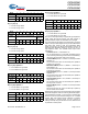
Bit # 7 6543210
Bit Name Device
Address
Enable
Device Address
Read/Write R/W R/W R/W R/W R/W R/W R/W R/W
Reset 0 0000000
Figure 14-1. USB Device Address Register (Address 0x10)
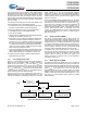
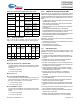
Bit # 765 4 3:0
Bit
Name
SETUP
Received
IN
Received
OUT
Received
ACKed
Transaction
Mode Bit
Read/
Write
R/W R/W R/W R/W R/W
Reset 0 0 0 0 0000
Figure 14-2. Endpoint 0 Mode Register (Address 0x12)