
User`s guide

CY7C63722C
CY7C63723C
CY7C63743C
FOR
FOR
Document #: 38-08022 Rev. *C Page 28 of 49
During a Watchdog Reset, the Processor Status and Control
Register is set to 01XX0001, which indicates a Watchdog
Reset (bit 4 set) has occurred and no interrupts are pending
(bit 7 clear).
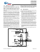
21.0 Interrupts
Interrupts can be generated by the GPIO lines, the internal
free-running timer, the SPI block, the capture timers, on
various USB events, PS/2 activity, or by the wake-up timer. All
interrupts are maskable by the Global Interrupt Enable
Register and the USB End Point Interrupt Enable Register.
Writing a ‘1’ to a bit position enables the interrupt associated
with that bit position. During a reset, the contents of the
interrupt enable registers are cleared, along with the Global
Interrupt enable bit of the CPU, effectively disabling all inter-
rupts.
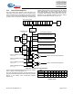
The interrupt controller contains a separate flip-flop for each
interrupt. See Figure 21-3 for the logic block diagram of the
interrupt controller. When an interrupt is generated it is first
registered as a pending interrupt. It will stay pending until it is
serviced or a reset occurs. A pending interrupt will only
generate an interrupt request if it is enabled by the corre-
sponding bit in the interrupt enable registers. The highest
priority interrupt request will be serviced following the
completion of the currently executing instruction.
When servicing an interrupt, the hardware will first disable all
interrupts by clearing the Global Interrupt Enable bit in the
CPU (the state of this bit can be read at Bit 2 of the Processor
Status and Control Register). Next, the flip-flop of the current
interrupt is cleared. This is followed by an automatic CALL
instruction to the ROM address associated with the interrupt
being serviced (i.e., the Interrupt Vector, see Section 21.1).
The instruction in the interrupt table is typically a JMP
instruction to the address of the Interrupt Service Routine
(ISR). The user can re-enable interrupts in the interrupt service
routine by executing an EI instruction. Interrupts can be nested
to a level limited only by the available stack space.
The Program Counter value as well as the Carry and Zero
flags (CF, ZF) are stored onto the Program Stack by the
automatic CALL instruction generated as part of the interrupt
acknowledge process. The user firmware is responsible for
ensuring that the processor state is preserved and restored
during an interrupt. The PUSH A instruction should typically be
used as the first command in the ISR to save the accumulator
value and the POP A instruction should be used just before the
RETI instruction to restore the accumulator value. The
program counter, CF and ZF are restored and interrupts are
enabled when the RETI instruction is executed.
The DI and EI instructions can be used to disable and enable
interrupts, respectively. These instructions affect only the
Global Interrupt Enable bit of the CPU. If desired, EI can be
used to re-enable interrupts while inside an ISR, instead of
waiting for the RETI that exits the ISR. While the global
interrupt enable bit is cleared, the presence of a pending
interrupt can be detected by examining the IRQ Sense bit (Bit
7 in the Processor Status and Control Register).
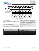
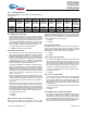
21.1 Interrupt Vectors
The Interrupt Vectors supported by the device are listed in
Table 21-1. The highest priority interrupt is #1 (USB Bus Reset
/ PS/2 activity), and the lowest priority interrupt is #11
(Wake-up Timer). Although Reset is not an interrupt, the first
instruction executed after a reset is at ROM address 0x0000,
which corresponds to the first entry in the Interrupt Vector
Table. Interrupt vectors occupy two bytes to allow for a
two-byte JMP instruction to the appropriate Interrupt Service
Routine (ISR).
21.2 Interrupt Latency
Interrupt latency can be calculated from the following
equation:
Interrupt Latency = (Number of clock cycles remaining in the
current instruction)
+ (10 clock cycles for the CALL
instruction)
+ (5 clock cycles for the JMP instruction)
For example, if a 5 clock cycle instruction such as JC is being
executed when an interrupt occurs, the first instruction of the
Interrupt Service Routine will execute a minimum of 16 clocks
(1+10+5) or a maximum of 20 clocks (5+10+5) after the
interrupt is issued. With a 6-MHz external resonator, internal
CPU clock speed is 12 MHz, so 20 clocks take 20/12 MHz =
1.67 µs.
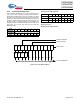
Table 21-1. Interrupt Vector Assignments
Interrupt Vec-
tor Number
ROM
Address Function
not applicable 0x0000 Execution after Reset begins
here
1 0x0002 USB Bus Reset or PS/2 Activity
interrupt
2 0x0004 128-µs timer interrupt
3 0x0006 1.024-ms timer interrupt
4 0x0008 USB Endpoint 0 interrupt
5 0x000A USB Endpoint 1 interrupt
6 0x000C USB Endpoint 2 interrupt
7 0x000E SPI Interrupt
8 0x0010 Capture Timer A interrupt
9 0x0012 Capture Timer B interrupt
10 0x0014 GPIO interrupt
11 0x0016 Wake-up Timer interrupt