
User`s guide

CY7C63722C
CY7C63723C
CY7C63743C
FOR
FOR
Document #: 38-08022 Rev. *C Page 40 of 49
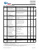
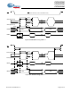
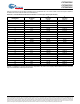
26.0 Switching Characteristics
Parameter Description Conditions Min. Max. Unit
Internal Clock Mode
F
ICLK
Internal Clock Frequency Internal Clock Mode enabled 5.7 6.3 MHz
F
ICLK2
Internal Clock Frequency, USB
mode
Internal Clock Mode enabled, Bit 2 of register
0xF8h is set (Precision USB Clocking)
[12]
5.91 6.09 MHz
External Oscillator Mode
T
CYC
Input Clock Cycle Time USB Operation, with External ±1.5%
Ceramic Resonator or Crystal
164.2 169.2 ns
T
CH
Clock HIGH Time 0.45 t
CYC
ns
T
CL
Clock LOW Time 0.45 t
CYC
ns
Reset Timing
t
START
Time-out Delay after LVR/BOR 24 60 ms
t
WAKE
Internal Wake-up Period Enabled Wake-up Interrupt
[13]
15ms
t
WATCH
WatchDog Timer Period F
OSC
= 6 MHz 10.1 14.6 ms
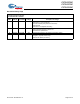
USB Driver Characteristics
T
R
Transition Rise Time CLoad = 200 pF (10% to 90%
[4]
)75 ns
T
R
Transition Rise Time CLoad = 600 pF (10% to 90%
[4]
) 300 ns
T
F
Transition Fall Time CLoad = 200 pF (10% to 90%
[4]
)75 ns
T
F
Transition Fall Time CLoad = 600 pF (10% to 90%
[4]
) 300 ns
T
RFM
Rise/Fall Time Matching t
r
/t
f
[4, 14]
80 125 %
V
CRS
Output Signal Crossover
Voltage
[18]
CLoad = 200 to 600 pF
[4]
1.3 2.0 V
USB Data Timing
T
DRATE
Low Speed Data Rate Ave. Bit Rate (1.5 Mb/s ±1.5%) 1.4775 1.5225 Mb/s
T
DJR1
Receiver Data Jitter Tolerance To Next Transition
[15]
–75 75 ns
T
DJR2
Receiver Data Jitter Tolerance For Paired Transitions
[15]
–45 45 ns
T
DEOP
Differential to EOP transition Skew Note 15 –40 100 ns
T
EOPR2
EOP Width at Receiver Accepts as EOP
[15]
670 ns
T
EOPT
Source EOP Width 1.25 1.50 µs
T
UDJ1
Differential Driver Jitter To next transition, Figure 26-5 –95 95 ns
T
UDJ2
Differential Driver Jitter To paired transition, Figure 26-5 –150 150 ns
T
LST
Width of SE0 during Diff. Transition 210 ns
Non-USB Mode Driver
Characteristics
Note 16
T
FPS2
SDATA/SCK Transition Fall Time CLoad = 150 pF to 600 pF 50 300 ns
SPI Timing See Figures 26-6 to 26-9
[17]
T
SMCK
SPI Master Clock Rate F
CLK
/3; see Figure 17-1 2MHz
T
SSCK
SPI Slave Clock Rate 2.2 MHz
Notes:
12. Initially F
ICLK2
= F
ICLK
until a USB packet is received.
13. Wake-up time for Wake-up Adjust Bits cleared to 000b (minimum setting)
14. Tested at 200 pF.
15. Measured at cross-over point of differential data signals.
16. Non-USB Mode refers to driving the D–/SDATA and/or D+/SCLK pins with the Control Bits of the USB Status and Control Register, with Control Bit 2 HIGH.
17. SPI timing specified for capacitive load of 50 pF, with GPIO output mode = 01 (medium low drive, strong high drive).
18. Per the USB 2.0 Specification, Table 7.7, Note 10, the first transition from the Idle state is excluded.