
User manual

CY8C21634/CY8C21534
CY8C21434/CY8C21334/CY8C21234
Document Number: 38-12025 Rev. *R Page 21 of 46
DC Operational Amplifier Specifications
The following tables list the guaranteed maximum and minimum specifications for the voltage and temperature ranges: 4.75V to 5.25V
and -40°C ≤ T
A
≤ 85°C, 3.0V to 3.6V and -40°C ≤ T
A
≤ 85°C, or 2.4V to 3.0V and -40°C ≤ T
A
≤ 85°C, respectively. Typical parameters
apply to 5V, 3.3V, or 2.7V at 25°C and are for design guidance only.
V
IH
Input High Level 2.1 – V Vdd = 3.0 to 5.25.
V
H
Input Hysteresis – 60 – mV
I
IL
Input Leakage (Absolute Value) – 1 – nA Gross tested to 1 μA.
C
IN
Capacitive Load on Pins as Input – 3.5 10 pF Package and pin dependent.
Temp = 25
o
C.
C
OUT
Capacitive Load on Pins as Output – 3.5 10 pF Package and pin dependent.
Temp = 25
o
C.
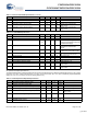
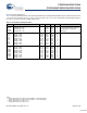
Table 13. 5V and 3.3V DC GPIO Specifications (continued)
Symbol Description Min Typ Max Units Notes
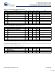
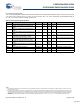
Table 14. 2.7V DC GPIO Specifications
Symbol Description Min Typ Max Units Notes
R
PU
Pull up Resistor 4 5.6 8 kΩ
R
PD
Pull down Resistor 4 5.6 8 kΩ
V
OH
High Output Level Vdd -
0.4
– – V IOH = 2.5 mA (6.25 Typ), Vdd = 2.4
to 3.0V (16 mA maximum, 50 mA Typ
combined IOH budget).
V
OL
Low Output Level – – 0.75 V IOL = 10 mA, Vdd = 2.4 to 3.0V (90
mA maximum combined IOL
budget).
I
OH
High Level Source Current 2.5 – – mA V
OH
= Vdd-0.4V, see the limitations of
the total current in the note for VOH
I
OL
Low Level Sink Current 10 – – mA V
OL
= 0.75V, see the limitations of the
total current in the note for VOL
V
IL
Input Low Level – – 0.75 V Vdd = 2.4 to 3.0.
V
IH
Input High Level 2.0 – – V Vdd = 2.4 to 3.0.
V
H
Input Hysteresis – 90 – mV
I
IL
Input Leakage (Absolute Value) – 1 – nA Gross tested to 1 μA.
C
IN
Capacitive Load on Pins as Input – 3.5 10 pF Package and pin dependent.
Temp = 2 5
o
C.
C
OUT
Capacitive Load on Pins as Output – 3.5 10 pF Package and pin dependent.
Temp = 2 5
o
C.
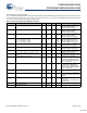
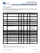
Table 15. 5V DC Operational Amplifier Specifications
Symbol Description Min Typ Max Units Notes
V
OSOA
Input Offset Voltage (absolute value) – 2.5 15 mV
TCV
OSOA
Average Input Offset Voltage Drift – 10 – μV/
o
C
I
EBOA
Input Leakage Current (Port 0 Analog Pins 7:1) – 200 – pA Gross tested to 1 μA.
I
EBOA00
Input Leakage Current (Port 0, Pin 0 Analog pin) – 50 – nA Gross tested to 1 μA.
C
INOA
Input Capacitance (Port 0 Analog Pins) – 4.5 9.5 pF Package and pin dependent.
Temp = 2 5
o
C.
V
CMOA
Common Mode Voltage Range 0.0 – Vdd - 1 V
G
OLOA
Open Loop Gain – 80 – dB
I
SOA
Amplifier Supply Current – 10 30 μA
[+] Feedback