
User manual

CY8C21634/CY8C21534
CY8C21434/CY8C21334/CY8C21234
Document Number: 38-12025 Rev. *R Page 27 of 46
AC Electrical Characteristics
AC Chip-Level Specifications
The following tables list the guaranteed maximum and minimum specifications for the voltage and temperature ranges: 4.75V to 5.25V
and -40°C ≤ T
A
≤ 85°C, 3.0V to 3.6V and -40°C ≤ T
A
≤ 85°C, or 2.4V to 3.0V and -40°C ≤ T
A
≤ 85°C, respectively. Typical parameters
apply to 5V, 3.3V, or 2.7V at 25°C and are for design guidance only.
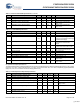
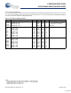
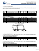
Table 23. 5V and 3.3V AC Chip-Level Specifications
Symbol Description Min Typ Max Units Notes
F
IMO24
Internal Main Oscillator Frequency for 24
MHz
23.4 24 24.6
[12,13,14]
MHz Trimmed for 5V or 3.3V
operation using factory trim
values. See Figure 14 on
page 18. SLIMO mode = 0.
F
IMO6
Internal Main Oscillator Frequency for 6 MHz 5.5 6 6.5
[12,13,14]
MHz Trimmed for 5V or 3.3V
operation using factory trim
values. See Figure 14 on
page 18. SLIMO mode = 1.
F
CPU1
CPU Frequency (5V Nominal) 0.93 24 24.6
[12,13]
MHz 24 MHz only for SLIMO
mode = 0.
F
CPU2
CPU Frequency (3.3V Nominal) 0.93 12 12.3
[13,14]
MHz
F
BLK5
Digital PSoC Block Frequency
0
(5V Nominal) 0 48 49.2
[12,13,15]
MHz Refer to AC Digital Block
Specifications on page 31.
F
BLK33
Digital PSoC Block Frequency (3.3V
Nominal)
0 24 24.6
[13,15]
MHz
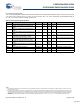
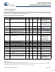
F
32K1
Internal Low Speed Oscillator Frequency 15 32 64 kHz
F
32K_U
Internal Low Speed Oscillator (ILO)
Untrimmed Frequency
5 – – kHz After a reset and before the
m8c starts to run, the ILO is
not trimmed. See the
System Resets section of
the PSoC Technical
Reference Manual for
details on this timing.
Jitter32k 32 kHz RMS Period Jitter – 100 200 ns
Jitter32k 32 kHz Peak-to-Peak Period Jitter – 1400 –
T
XRST
External Reset Pulse Width 10 – – μs
DC24M 24 MHz Duty Cycle 40 50 60 %
DC
ILO
Internal Low Speed Oscillator Duty Cycle 20 50 80 %
Step24M 24 MHz Trim Step Size – 50 – kHz
Fout48M 48 MHz Output Frequency 46.8 48.0 49.2
[12,14]
MHz Trimmed. Using factory trim
values.
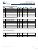
Jitter24M1 24 MHz Peak-to-Peak Period Jitter (IMO) – 600 ps
F
MAX
Maximum frequency of signal on row input
or row output.
– – 12.3 MHz
SR
POWER_UP
Power Supply Slew Rate – – 250 V/ms Vdd slew rate during power
up.
T
POWERUP
Time from end of POR to CPU executing
code
– 16 100 ms Power up from 0V. See the
System Resets section of
the PSoC Technical
Reference Manual.
Notes
12. 4.75V < Vdd < 5.25V.
13. Accuracy derived from Internal Main Oscillator with appropriate trim for Vdd range.
14. 3.0V < Vdd < 3.6V. See Application Note AN2012 “Adjusting PSoC Microcontroller Trims for Dual Voltage-Range Operation” for information on trimming for operation
at 3.3V.
15. See the individual user module data sheets for information on maximum frequencies for user modules.
[+] Feedback