
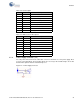
Specifications

CY3214-PSoCEVALUSB Kit Guide, Doc No. 001-67030 Rev. *B 21
Hardware
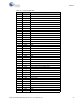
15 P1[7]
I
2
C serial clock (SCL)
16 P1[5]
I
2
C serial data (SCA)
17 P1[3] GPIO
18 P1[1]
I
2
C serial clock (SCL), ISSP SCLK[2]
19 Vss Ground connection
20 D+ GPIO
21 D– GPIO
22 Vdd Supply voltage
23 P7[7] GPIO
24 P7[0] GPIO
25 P1[0]
I
2
C serial data (SDA), ISSP SDATA[2]
26 P1[2] GPIO
27 P1[4] Optional external clock input (EXTCLK)
28 P1[6] GPIO
29 P5[0] GPIO
30 P5[2] GPIO
31 P5[4] GPIO
32 P5[6] GPIO
33 P3[0] GPIO
34 P3[2 GPIO
35 P3[4] GPIO
36 P3[6] GPIO
37 P4[0] GPIO
38 P4[2] GPIO
39 P4[4] GPIO
40 P4[6] GPIO
41 P2[0] Direct switched capacitor block input
42 P2[2] Direct switched capacitor block input
43 P2[4] External analog ground (AGND) input
44 P2[6] External voltage reference (VREF) input
45 P0[0] Analog column mux input
46 P0[2] Analog column mux input
47 P0[4] Analog column mux input VREF
48 P0[6] Analog column mux input
49 Vdd Supply voltage
50 Vss Ground connection
51 P0[7] Analog column mux input
52 P0[5] Analog column mux input and column output
53 P0[3] Analog column mux input and column output
54 P0[1] Analog column mux input
55 P2[7] GPIO
56 P2[5] GPIO
Table 4-1. Functional Pin Table
Pin No. Pin Name Description