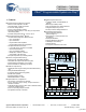
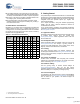
CY8C29466, CY8C29566 CY8C29666, CY8C29866 PSoC® Programmable System-on-Chip™ 1. Features ■ ■ ■ ■ ■ Powerful Harvard Architecture Processor ❐ M8C Processor Speeds to 24 MHz ❐ Two 8x8 Multiply, 32-Bit Accumulate ❐ Low Power at High Speed ❐ 3.0V to 5.25V Operating Voltage ❐ Operating Voltages Down to 1.
CY8C29466, CY8C29566 CY8C29666, CY8C29866 3. Contents Features............................................................................... 1 Logic Block Diagram.......................................................... 1 Contents .............................................................................. 2 PSoC Functional Overview................................................ 3 PSoC Core .................................................................... 3 Digital System ..........................
CY8C29466, CY8C29566 CY8C29666, CY8C29866 4. PSoC Functional Overview The PSoC family consists of many Programmable System-on-Chip Controller devices. These devices are designed to replace multiple traditional MCU-based system components with one, low cost single-chip programmable device. PSoC devices include configurable blocks of analog and digital logic, as well as programmable interconnects.
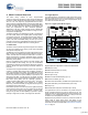
CY8C29466, CY8C29566 CY8C29666, CY8C29866 Figure 4-2. Analog System Block Diagram The Analog System is composed of 12 configurable blocks, each comprised of an opamp circuit allowing the creation of complex analog signal flows. Analog peripherals are very flexible and can be customized to support specific application requirements. Some of the more common PSoC analog functions (most available as user modules) are listed below.
CY8C29466, CY8C29566 CY8C29666, CY8C29866 ■ ■ ■ Low Voltage Detection (LVD) interrupts can signal the application of falling voltage levels, while the advanced POR (Power On Reset) circuit eliminates the need for a system supervisor. An internal 1.3V reference provides an absolute reference for the analog system, including ADCs and DACs. An integrated switch mode pump (SMP) generates normal operating voltages from a single 1.2V battery cell, providing a low cost boost converter. 4.
CY8C29466, CY8C29566 CY8C29666, CY8C29866 6. Development Tools PSoC Designer is a Microsoft® Windows-based, integrated development environment for the Programmable System-on-Chip (PSoC) devices. The PSoC Designer IDE runs on Windows XP or Windows Vista. This system provides design database management by project, an integrated debugger with In-Circuit Emulator, in-system programming support, and built in support for third party assemblers and C compilers.
CY8C29466, CY8C29566 CY8C29666, CY8C29866 7. Designing with PSoC Designer The development process for the PSoC device differs from that of a traditional fixed function microprocessor. The configurable analog and digital hardware blocks give the PSoC architecture a unique flexibility that pays dividends in managing specification change during development and by lowering inventory costs.
CY8C29466, CY8C29566 CY8C29666, CY8C29866 8. Document Conventions 8.2 Units of Measure 8.1 Acronyms Used This table lists the acronyms used in this data sheet. A units of measure table is located in the section Electrical Specifications on page 20. Table 12-1 on page 20 lists all the abbreviations used to measure the PSoC devices. Table 8-1. Acronyms 8.
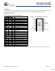
CY8C29466, CY8C29566 CY8C29666, CY8C29866 9. Pinouts The CY8C29x66 PSoC device is available in a variety of packages which are listed and illustrated in the following tables. Every port pin (labeled with a “P”) is capable of Digital I/O. However, Vss, Vdd, SMP, and XRES are not capable of Digital I/O. 9.1 28-Pin Part Pinout Table 9-1. 28-Pin Part Pinout (PDIP, SSOP, SOIC) Pin No.
CY8C29466, CY8C29566 CY8C29666, CY8C29866 9.2 44-Pin Part Pinout Table 9-2.
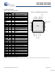
CY8C29466, CY8C29566 CY8C29666, CY8C29866 9.3 48-Pin Part Pinouts Table 9-3. 48-Pin Part Pinout (SSOP) Pin No.
CY8C29466, CY8C29566 CY8C29666, CY8C29866 Table 9-4. 48-Pin Part Pinout (QFN)** I/O I P2[3] Direct switched capacitor block input. 2 I/O I P2[1] Direct switched capacitor block input. 3 I/O P4[7] 4 I/O P4[5] 5 I/O P4[3] 6 I/O SMP Switch Mode Pump (SMP) connection to external components required. 8 I/O P3[7] 9 I/O P3[5] 10 I/O P3[3] 11 I/O P3[1] 12 I/O P5[3] 13 I/O P5[1] 14 I/O P1[7] I2C Serial Clock (SCL). 15 I/O P1[5] I2C Serial Data (SDA).
CY8C29466, CY8C29566 CY8C29666, CY8C29866 9.4 100-Pin Part Pinout Table 9-5. 100-Pin Part Pinout (TQFP) Pin No.
CY8C29466, CY8C29566 CY8C29666, CY8C29866 77 76 Vdd Vdd P0[6], A, I NC P0[4], A, IO NC P0[2], A, IO NC P6[7] P6[6] P6[5] P6[4] P6[3] P6[2] P6[1] P6[0] Vss Vss TQFP 75 74 73 72 71 70 69 68 67 66 65 64 63 62 61 60 59 58 57 56 55 54 53 52 51 26 27 28 29 30 31 32 33 34 35 36 37 38 39 40 41 42 43 44 45 46 47 48 49 50 1 2 3 4 5 6 7 8 9 10 11 12 13 14 15 16 17 18 19 20 21 22 23 24 25 NC P0[0], A, I NC P2[6],External VREF NC P2[4],External AGND P2[2], A, I P2[0], A, I P4[6] P4[4] Vss P4[2] P4[0] XRES NC NC
CY8C29466, CY8C29566 CY8C29666, CY8C29866 9.5 100-Pin Part Pinout (On-Chip Debug) The 100-pin TQFP part is for the CY8C29000 On-Chip Debug (OCD) PSoC device. Note OCD parts are only used for in-circuit debugging.
CY8C29466, CY8C29566 CY8C29666, CY8C29866 77 76 Vdd Vdd P0[6], AI NC P0[4], AIO NC P0[2], AIO NC 87 86 85 84 83 82 81 80 79 78 90 89 88 P6[7] P6[6] P6[5] P6[4] P6[3] P6[2] P6[1] P6[0] Vss Vss 98 97 96 95 94 93 92 91 OCD TQFP 75 74 73 72 71 70 69 68 67 66 65 64 63 62 61 60 59 58 57 56 55 Document Number: 38-12013 Rev.
CY8C29466, CY8C29566 CY8C29666, CY8C29866 This section lists the registers of the CY8C29x66 PSoC device. For detailed register information, reference the PSoC Programmable System-on-Chip Technical Reference Manual. 10. Register Conventions 11. Register Mapping Tables 10.1 Abbreviations Used The PSoC device has a total register address space of 512 bytes. The register space is referred to as I/O space and is divided into two banks.
CY8C29466, CY8C29566 CY8C29666, CY8C29866 Table 11-1.
CY8C29466, CY8C29566 CY8C29666, CY8C29866 Table 11-2.
CY8C29466, CY8C29566 CY8C29666, CY8C29866 12. Electrical Specifications This section presents the DC and AC electrical specifications of the CY8C29x66 PSoC device. For the most up to date electrical specifications, confirm that you have the most recent data sheet by going to the web at http://www.cypress.com/psoc. Specifications are valid for -40°C ≤ TA ≤ 85°C and TJ ≤ 100°C, except where noted. Refer to Table 12-17 for the electrical specifications on the internal main oscillator (IMO) using SLIMO mode.
CY8C29466, CY8C29566 CY8C29666, CY8C29866 12.1 Absolute Maximum Ratings Exceeding maximum ratings may shorten the useful life of the device. User guidelines are not tested. Table 12-2. Absolute Maximum Ratings Symbol Description Min Typ Max Unit Notes Higher storage temperatures reduce data retention time. Recommended storage temperature is +25°C ± 25°C. Extended duration storage temperatures above 65oC degrade reliability.
CY8C29466, CY8C29566 CY8C29666, CY8C29866 12.3 DC Electrical Characteristics 12.3.1 DC Chip-Level Specifications The following table lists guaranteed maximum and minimum specifications for the voltage and temperature ranges: 4.75V to 5.25V and -40°C ≤ TA ≤ 85°C, or 3.0V to 3.6V and -40°C ≤ TA ≤ 85°C, respectively. Typical parameters apply to 5V and 3.3V at 25°C and are for design guidance only. Table 12-4. DC Chip-Level Specifications Min Typ Max Units Notes Vdd Symbol Supply Voltage Description 3.
CY8C29466, CY8C29566 CY8C29666, CY8C29866 12.3.3 DC Operational Amplifier Specifications The following tables list guaranteed maximum and minimum specifications for the voltage and temperature ranges: 4.75V to 5.25V and -40°C ≤ TA ≤ 85°C, or 3.0V to 3.6V and -40°C ≤ TA ≤ 85°C, respectively. Typical parameters apply to 5V and 3.3V at 25°C and are for design guidance only. The Operational Amplifier is a component of both the Analog Continuous Time PSoC blocks and the Analog Switched Cap PSoC blocks.
CY8C29466, CY8C29566 CY8C29666, CY8C29866 12.3.4 DC Low Power Comparator Specifications The following table lists guaranteed maximum and minimum specifications for the voltage and temperature ranges: 4.75V to 5.25V and -40°C ≤ TA ≤ 85°C, 3.0V to 3.6V and -40°C ≤ TA ≤ 85°C, or 2.4V to 3.0V and -40°C ≤ TA ≤ 85°C, respectively. Typical parameters apply to 5V at 25°C and are for design guidance only. Table 12-8. DC Low Power Comparator Specifications Symbol Description Min Typ Max 0.
CY8C29466, CY8C29566 CY8C29666, CY8C29866 Table 12-10. 3.3V DC Analog Output Buffer Specifications Min Typ Max VOSOB Symbol Input Offset Voltage (Absolute Value) – 3 12 mV TCVOSOB Average Input Offset Voltage Drift – +6 – μV/°C VCMOB Common-Mode Input Voltage Range 0.5 - Vdd - 1.0 V ROUTOB Output Resistance Power = Low Power = High – – – – 10 10 W W VOHIGHOB High Output Voltage Swing (Load = 1k ohms to Vdd/2) Power = Low Power = High 0.5 x Vdd + 1.0 0.5 x Vdd + 1.
CY8C29466, CY8C29566 CY8C29666, CY8C29866 Figure 12-3. Basic Switch Mode Pump Circuit D1 Vdd L1 V BAT + V PUMP C1 SMP Battery PSoC Vss 12.3.7 DC Analog Reference Specifications The following tables list guaranteed maximum and minimum specifications for the voltage and temperature ranges: 4.75V to 5.25V and -40°C ≤ TA ≤ 85°C, or 3.0V to 3.6V and -40°C ≤ TA ≤ 85°C, respectively. Typical parameters apply to 5V and 3.3V at 25°C and are for design guidance only.
CY8C29466, CY8C29566 CY8C29666, CY8C29866 Table 12-13. 3.3V DC Analog Reference Specifications Symbol Description VBG33 Bandgap Voltage Reference 3.3V Min 1.28 Typ 1.30 Max 1.32 Unit – AGND = Vdd/2[4] Vdd/2 - 0.02 Vdd/2 Vdd/2 + 0.02 – – AGND = 2 x BandGap[4] AGND = P2[4] (P2[4] = Vdd/2) P2[4] - 0.009 Not Allowed P2[4] P2[4] + 0.009 – AGND = BandGap[4] – AGND = 1.
CY8C29466, CY8C29566 CY8C29666, CY8C29866 Table 12-15. DC POR, SMP, and LVD Specifications (continued) Symbol Min Typ Max Units VLVD0 VLVD1 VLVD2 VLVD3 VLVD4 VLVD5 VLVD6 VLVD7 Vdd Value for LVD Trip VM[2:0] = 000b VM[2:0] = 001b VM[2:0] = 010b VM[2:0] = 011b VM[2:0] = 100b VM[2:0] = 101b VM[2:0] = 110b VM[2:0] = 111b Description 2.86 2.96 3.07 3.92 4.39 4.55 4.63 4.72 2.92 3.02 3.13 4.00 4.48 4.64 4.73 4.81 2.98[5] 3.08 3.20 4.08 4.57 4.74[6] 4.82 4.
CY8C29466, CY8C29566 CY8C29666, CY8C29866 12.4 AC Electrical Characteristics 12.4.1 AC Chip-Level Specifications The following table lists guaranteed maximum and minimum specifications for the voltage and temperature ranges: 4.75V to 5.25V and -40°C ≤ TA ≤ 85°C, or 3.0V to 3.6V and -40°C ≤ TA ≤ 85°C, respectively. Typical parameters apply to 5V and 3.3V at 25°C and are for design guidance only. Note See the individual user module data sheets for information on maximum frequencies for user modules.
CY8C29466, CY8C29566 CY8C29666, CY8C29866 Table 12-17. AC Chip-Level Specifications (continued) Symbol Description Min Typ Max Units 20 50 80 % DCILO Internal Low Speed Oscillator Duty Cycle Step24M 24 MHz Trim Step Size – 50 – kHz Fout48M 48 MHz Output Frequency 46.8 48.0 49.2[9, 11] MHz Jitter24M1 24 MHz Period Jitter (IMO) – 600 – ps FMAX Maximum frequency of signal on row input or row output. – – 12.
CY8C29466, CY8C29566 CY8C29666, CY8C29866 12.4.2 AC General Purpose I/O Specifications The following table lists guaranteed maximum and minimum specifications for the voltage and temperature ranges: 4.75V to 5.25V and -40°C ≤ TA ≤ 85°C, or 3.0V to 3.6V and -40°C ≤ TA ≤ 85°C, respectively. Typical parameters apply to 5V and 3.3V at 25°C and are for design guidance only. Table 12-18. AC GPIO Specifications Symbol Min Typ Max Unit GPIO Operating Frequency 0 – 12.
CY8C29466, CY8C29566 CY8C29666, CY8C29866 Table 12-20. 3.3V AC Operational Amplifier Specifications Symbol TROA TSOA SRROA SRFOA Description Rising Settling Time to 0.1% of a 1V Step (10 pF load, Unity Gain) Power = Low, Opamp Bias = Low Power = Medium, Opamp Bias = High Falling Settling Time to 0.
CY8C29466, CY8C29566 CY8C29666, CY8C29866 Figure 12-11. Typical Opamp Noise nV/rtHz 10000 PH_BH PH_BL PM_BL PL_BL 1000 100 10 0.001 0.01 0.1 Freq (kHz) 1 10 100 12.4.4 AC Low Power Comparator Specifications The following table lists guaranteed maximum and minimum specifications for the voltage and temperature ranges: 4.75V to 5.25V and -40°C ≤ TA ≤ 85°C, 3.0V to 3.6V and -40°C ≤ TA ≤ 85°C, or 2.4V to 3.0V and -40°C ≤ TA ≤ 85°C, respectively.
CY8C29466, CY8C29566 CY8C29666, CY8C29866 Table 12-22. AC Digital Block Specifications (continued) Min Typ Max Unit CRCPRS Maximum Input Clock Frequency (PRS Mode) Function Description – – 49.2 MHz 4.75V < Vdd < 5.25V. Notes CRCPRS Maximum Input Clock Frequency (CRC Mode) – – 24.6 MHz SPIM Maximum Input Clock Frequency – – 8.2 MHz Maximum data rate at 4.1 MHz due to 2 x over clocking. SPIS Maximum Input Clock Frequency – – 4.
CY8C29466, CY8C29566 CY8C29666, CY8C29866 12.4.7 AC External Clock Specifications The following tables list guaranteed maximum and minimum specifications for the voltage and temperature ranges: 4.75V to 5.25V and -40°C ≤ TA ≤ 85°C, or 3.0V to 3.6V and -40°C ≤ TA ≤ 85°C, respectively. Typical parameters apply to 5V and 3.3V at 25°C and are for design guidance only. Table 12-25. 5V AC External Clock Specifications Min Typ Max Unit FOSCEXT Symbol Frequency Description 0.093 – 24.
CY8C29466, CY8C29566 CY8C29666, CY8C29866 12.4.9 AC I2C Specifications The following table lists guaranteed maximum and minimum specifications for the voltage and temperature ranges: 4.75V to 5.25V and -40°C ≤ TA ≤ 85°C, or 3.0V to 3.6V and -40°C ≤ TA ≤ 85°C, respectively. Typical parameters apply to 5V and 3.3V at 25°C and are for design guidance only. Table 12-28.
CY8C29466, CY8C29566 CY8C29666, CY8C29866 13. Packaging Information This section illustrates the packaging specifications for the CY8C29x66 PSoC device, along with the thermal impedances for each package and the typical package capacitance on crystal pins. Important Note Emulation tools may require a larger area on the target PCB than the chip’s footprint. For a detailed description of the emulation tools’ dimensions, refer to the document titled PSoC Emulator Pod Dimensions at http://www.cypress.
CY8C29466, CY8C29566 CY8C29666, CY8C29866 Figure 13-2. 28-Pin (210-Mil) SSOP 51-85079 *C 51-85079 *D Figure 13-3. 28-Pin (300-Mil) SOIC 51-85026 *D Document Number: 38-12013 Rev.
CY8C29466, CY8C29566 CY8C29666, CY8C29866 Figure 13-4. 44-Pin TQFP 51-85064 *C Figure 13-5. 48-Pin (7x7 mm) QFN SIDE VIEW TOP VIEW BOTTOM VIEW 0.08 C 1.00 MAX. 6.90 7.10 0.05 MAX. 5.1 0.80 MAX. 6.70 6.80 0.23±0.05 0.20 REF. N N PIN1 ID 0.20 R. 1 2 0.45 1 2 0.80 DIA. 6.70 6.80 6.90 7.10 5.1 SOLDERABLE EXPOSED PAD 5.45 5.55 0.30-0.45 0°-12° NOTES: 1. 0.42±0.18 (4X) 0.50 C SEATING PLANE 5.45 5.55 HATCH AREA IS SOLDERABLE EXPOSED METAL. 2. REFERENCE JEDEC#: MO-220 3.
CY8C29466, CY8C29566 CY8C29666, CY8C29866 Figure 13-6. 48-Pin (300-Mil) SSOP 51-85061 *C 51-85061-C Figure 13-7. 48-Pin QFN 7x7x 0.90 MM (Sawn Type) TOP VIEW SIDE VIEW 7.00±0.100 48 BOTTOM VIEW 0.900±0.100 0.25 36 1 5.100 REF 0.200 REF. 37 0.50 PITCH +0.05 -0.07 PIN1 ID R 0.20 37 PIN 1 DOT 1 36 LASER MARK 0.45 7.00±0.100 SOLDERABLE EXPOSED PAD 5.100 REF 12 25 13 24 C HATCH AREA IS SOLDERABLE EXPOSED METAL. 0.08 NOTES: SEATING PLANE 0.020 +0.025 -0.00 1. 5.500±0.
CY8C29466, CY8C29566 CY8C29666, CY8C29866 Figure 13-8. 100-Pin TQFP 51-85048 ** 51-85048 *C Important Note For information on the preferred dimensions for mounting QFN packages, see the following Application Note at http://www.amkor.com/products/notes_papers/MLFAppNote.pdf. Important Note Pinned vias for thermal conduction are not required for the low-power PSoC device. Document Number: 38-12013 Rev.
CY8C29466, CY8C29566 CY8C29666, CY8C29866 13.1 Thermal Impedances 13.2 Capacitance on Crystal Pins Table 13-1. Thermal Impedances per Package Table 13-2. Typical Package Capacitance on Crystal Pins Package Typical θJA * Package Package Capacitance 28 PDIP 69 oC/W 28 PDIP 3.5 pF 28 SSOP 94 oC/W 28 SSOP 2.8 pF 28 SOIC 67 oC/W 28 SOIC 2.7 pF 44 TQFP 60 oC/W 44 TQFP 2.6 pF 48 SSOP 69 oC/W 48 SSOP 3.3 pF 48 QFN** 28 oC/W 48 QFN 1.8 pF 100 TQFP 50 oC/W 100 TQFP 3.
CY8C29466, CY8C29566 CY8C29666, CY8C29866 14. Development Tool Selection ■ iMAGEcraft C Compiler (Registration Required) ■ ISSP Cable ■ USB 2.0 Cable and Blue Cat-5 Cable 14.1 Software ■ 2 CY8C29466-24PXI 28-PDIP Chip Samples 14.1.1 PSoC Designer™ 14.3 Evaluation Tools At the core of the PSoC development software suite is PSoC Designer, used to generate PSoC firmware applications. PSoC Designer is available free of charge at http://www.cypress.com/psocdesigner and includes a free C compiler.
CY8C29466, CY8C29566 CY8C29666, CY8C29866 14.3.3 CY3214-PSoCEvalUSB The CY3214-PSoCEvalUSB evaluation kit features a development board for the CY8C24794-24LFXI PSoC device. Special features of the board include both USB and capacitive sensing development and debugging support. This evaluation board also includes an LCD module, potentiometer, LEDs, an enunciator and plenty of bread boarding space to meet all of your evaluation needs.
CY8C29466, CY8C29566 CY8C29666, CY8C29866 16.
CY8C29466, CY8C29566 CY8C29666, CY8C29866 18. Document History Page Document Title: CY8C29466, CY8C29566, CY8C29666, and CY8C29866 PSoC®Programmable System-on-Chip Document Number: 38-12013 Revision ECN No. Submission Date Origin of Change Description of Change ** 131151 11/13/2003 New Silicon New document (Revision **). *A 132848 01/21/2004 NWJ New information. First edition of preliminary data sheet. *B 133205 01/27/2004 NWJ Changed part numbers, increased SRAM data storage to 2K bytes.
CY8C29466, CY8C29566 CY8C29666, CY8C29866 19. Sales, Solutions, and Legal Information 19.1 Worldwide Sales and Design Support Cypress maintains a worldwide network of offices, solution centers, manufacturer’s representatives, and distributors. To find the office closest to you, visit us at Cypress Locations. 19.2 Products Automotive Clocks & Buffers Interface Lighting & Power Control 19.3 PSoC Solutions cypress.com/go/automotive psoc.cypress.com/solutions cypress.