
User manual

CY8C29466, CY8C29566
CY8C29666, CY8C29866
Document Number: 38-12013 Rev. *M Page 15 of 47
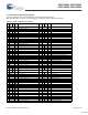
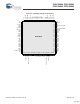
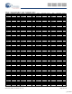
9.5 100-Pin Part Pinout (On-Chip Debug)
The 100-pin TQFP part is for the CY8C29000 On-Chip Debug (OCD) PSoC device.
Note OCD parts are only used for in-circuit debugging. OCD parts are NOT available for production
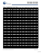
Table 9-6. 100-Pin OCD Part Pinout (TQFP)
Pin
No.
Digital
Analog
Name Description
Pin
No.
Digital
Analog
Name Description
1 NC No internal connection. 51 NC No internal connection.
2 NC No internal connection. 52 I/O P5[0]
3 I/O I P0[1] Analog column mux input. 53 I/O P5[2]
4 I/O P2[7] 54 I/O P5[4]
5 I/O P2[5] 55 I/O P5[6]
6 I/O I P2[3] Direct switched capacitor block input. 56 I/O P3[0]
7 I/O I P2[1] Direct switched capacitor block input. 57 I/O P3[2]
8 I/O P4[7] 58 I/O P3[4]
9 I/O P4[5] 59 I/O P3[6]
10 I/O P4[3] 60 HCLK OCD high speed clock output
11 I/O P4[1] 61 CCLK OCD CPU clock output
12 OCDE OCD even data I/O 62 Input XRES Active high pin reset with internal pull down.
13 OCDO OCD odd data output 63 I/O P4[0]
14 Power SMP Switch Mode Pump (SMP) connection to
required external components.
64 I/O P4[2]
15 Power Vss Ground connection. 65 Power Vss Ground connection.
16 I/O P3[7] 66 I/O P4[4]
17 I/O P3[5] 67 I/O P4[6]
18 I/O P3[3] 68 I/O I P2[0] Direct switched capacitor block input.
19 I/O P3[1] 69 I/O I P2[2] Direct switched capacitor block input.
20 I/O P5[7] 70 I/O P2[4] External Analog Ground (AGND) input.
21 I/O P5[5] 71 NC No internal connection.
22 I/O P5[3] 72 I/O P2[6] External Voltage Reference (VREF) input.
23 I/O P5[1] 73 NC No internal connection.
24 I/O P1[7] I
2
C Serial Clock (SCL) 74 I/O I P0[0] Analog column mux input.
25 NC No internal connection. 75 NC No internal connection.
26 NC No internal connection. 76 NC No internal connection.
27 NC No internal connection. 77 I/O I/O P0[2] Analog column mux input and column output.
28 I/O P1[5] I
2
C Serial Data (SDA). 78 NC No internal connection.
29 I/O P1[3] I
FMTEST
79 I/O I/O P0[4] Analog column mux input and column output,
V
REF
.
30 I/O P1[1]* Crystal (XTALin), I
2
C Serial Clock (SCL), TC
SCLK.
80 NC No internal connection.
31 NC No internal connection. 81 I/O I P0[6] Analog column mux input.
32 Power Vdd Supply voltage. 82 Power Vdd Supply voltage.
33 NC No internal connection. 83 Power Vdd Supply voltage.
34 Power Vss Ground connection. 84 Power Vss Ground connection.
35 NC No internal connection. 85 Power Vss Ground connection.
36 I/O P7[7] 86 I/O P6[0]
37 I/O P7[6] 87 I/O P6[1]
38 I/O P7[5] 88 I/O P6[2]
39 I/O P7[4] 89 I/O P6[3]
40 I/O P7[3] 90 I/O P6[4]
41 I/O P7[2] 91 I/O P6[5]
42 I/O P7[1] 92 I/O P6[6]
43 I/O P7[0] 93 I/O P6[7]
44 I/O P1[0]* Crystal (XTALout), I
2
C Serial Data (SDA), TC
SDATA
94 NC No internal connection.
45 I/O P1[2] V
FMTEST
95 I/O I P0[7] Analog column mux input.
46 I/O P1[4] Optional External Clock Input (EXTCLK) 96 NC No internal connection.
47 I/O P1[6] 97 I/O I/O P0[5] Analog column mux input and column output.
48 NC No internal connection. 98 NC No internal connection.
49 NC No internal connection. 99 I/O I/O P0[3] Analog column mux input and column output.
50 NC No internal connection. 100 NC No internal connection.
LEGEND A = Analog, I = Input, O = Output, NC = No Connection, TC/TM: Test.
* ISSP pin which is not HiZ at POR.
[+] Feedback