
User manual

CY8C29466, CY8C29566
CY8C29666, CY8C29866
Document Number: 38-12013 Rev. *M Page 17 of 47
This section lists the registers of the CY8C29x66 PSoC device. For detailed register information, reference the
PSoC Programmable System-on-Chip Technical Reference Manual.
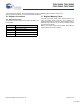
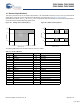
10. Register Conventions
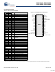
10.1 Abbreviations Used
The register conventions specific to this section are listed in the
following table.
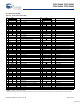
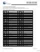
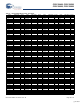
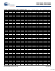
11. Register Mapping Tables
The PSoC device has a total register address space of 512
bytes. The register space is referred to as I/O space and is
divided into two banks. The XOI bit in the Flag register (CPU_F)
determines which bank the user is currently in. When the XOI bit
is set the user is in Bank 1.
Note In the following register mapping tables, blank fields are
reserved and should not be accessed.
Convention Description
R Read register or bit(s)
W Write register or bit(s)
L Logical register or bit(s)
C Clearable register or bit(s)
# Access is bit specific
[+] Feedback