
User manual

CY8C29466, CY8C29566
CY8C29666, CY8C29866
Document Number: 38-12013 Rev. *M Page 22 of 47
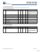
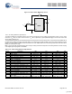
12.3 DC Electrical Characteristics
12.3.1 DC Chip-Level Specifications
The following table lists guaranteed maximum and minimum specifications for the voltage and temperature ranges: 4.75V to 5.25V
and -40°C ≤ T
A
≤ 85°C, or 3.0V to 3.6V and -40°C ≤ T
A
≤ 85°C, respectively. Typical parameters apply to 5V and 3.3V at 25°C and
are for design guidance only.
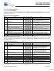
12.3.2 DC General Purpose I/O Specifications
The following table lists guaranteed maximum and minimum specifications for the voltage and temperature ranges: 4.75V to 5.25V
and -40°C ≤ T
A
≤ 85°C, or 3.0V to 3.6V and -40°C ≤ T
A
≤ 85°C, respectively. Typical parameters apply to 5V and 3.3V at 25°C and
are for design guidance only.
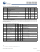
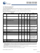
Table 12-4. DC Chip-Level Specifications
Symbol Description Min Typ Max Units Notes
Vdd Supply Voltage 3.00 – 5.25 V See DC POR, SMP, and LVD Specifications on page 27.
I
DD
Supply Current – 8 14 mA Conditions are 5.0V, T
A
= 25
o
C, CPU = 3 MHz,
SYSCLK doubler disabled, VC1 = 1.5 MHz,
VC2 = 93.75 kHz, VC3 = 0.366 kHz.
I
DD3
Supply Current – 5 9 mA Conditions are Vdd = 3.3V, T
A
= 25
o
C, CPU = 3 MHz,
SYSCLK doubler disabled, VC1 = 1.5 MHz, VC2 = 93.75
kHz, VC3 = 0.366 kHz.
I
DDP
Supply current when IMO = 6 MHz using SLIMO
mode.
– 2 3 mA Conditions are Vdd = 3.3V, T
A
= 25
o
C, CPU = 0.75 MHz,
SYSCLK doubler disabled,
VC1 = 0.375 MHz, VC2 = 23.44 kHz, VC3 = 0.09 kHz.
I
SB
Sleep (Mode) Current with POR, LVD, Sleep Timer,
WDT, and internal slow oscillator active.
– 3 10 μA Conditions are with internal slow speed oscillator,
Vdd = 3.3V, -40
o
C ≤ T
A
≤ 55
o
C.
I
SBH
Sleep (Mode) Current with POR, LVD, Sleep Timer,
WDT, and internal slow oscillator active.
– 4 25 μA Conditions are with internal slow speed oscillator,
Vdd = 3.3V, 55
o
C < T
A
≤ 85
o
C.
I
SBXTL
Sleep (Mode) Current with POR, LVD, Sleep Timer,
WDT, internal slow oscillator, and 32 kHz crystal
oscillator active.
– 4 12 μA Conditions are with properly loaded, 1 μW max,
32.768 kHz crystal. Vdd = 3.3V, -40
o
C ≤ T
A
≤ 55
o
C.
I
SBXTLH
Sleep (Mode) Current with POR, LVD, Sleep Timer,
WDT, and 32 kHz crystal oscillator active.
– 5 27 μA Conditions are with properly loaded, 1 μW max,
32.768 kHz crystal. Vdd = 3.3V, 55
o
C < T
A
≤ 85
o
C.
V
REF
Reference Voltage (Bandgap) 1.28 1.3 1.32 V Trimmed for appropriate Vdd.
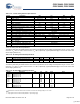
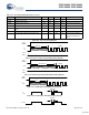
Table 12-5. DC GPIO Specifications
Symbol Description Min Typ Max Unit Notes
R
PU
Pull up Resistor 4 5.6 8 kΩ
R
PD
Pull down Resistor 4 5.6 8 kΩ
V
OH
High Output Level Vdd
- 1.0
––VI
OH
= 10 mA, Vdd = 4.75 to 5.25V (8 total loads,
4 on even port pins (for example, P0[2], P1[4]),
4 on odd port pins (for example, P0[3], P1[5])).
80 mA maximum combined I
OH
budget.
V
OL
Low Output Level – – 0.75 V I
OL
= 25 mA, Vdd = 4.75 to 5.25V (8 total loads,
4 on even port pins (for example, P0[2], P1[4]),
4 on odd port pins (for example, P0[3], P1[5])).
150 mA maximum combined I
OL
budget.
I
OH
High Level Source Current 10 – – mA V
OH
= Vdd-1.0V, see the limitations of the total current in
the note for VOH
I
OL
Low Level Sink Current 25 – – mA V
OL
= 0.75V, see the limitations of the total current in the
note for VOL
V
IL
Input Low Level – – 0.8 V Vdd = 3.0 to 5.25.
V
IH
Input High Level 2.1 – – V Vdd = 3.0 to 5.25.
V
H
Input Hysterisis – 60 – mV
I
IL
Input Leakage (Absolute Value) – 1 – nA Gross tested to 1 μA.
C
IN
Capacitive Load on Pins as Input – 3.5 10 pF Package and pin dependent. Temp = 25
o
C.
C
OUT
Capacitive Load on Pins as Output – 3.5 10 pF Package and pin dependent. Temp = 25
o
C.
[+] Feedback