
User manual

CY8C29466, CY8C29566
CY8C29666, CY8C29866
Document Number: 38-12013 Rev. *M Page 23 of 47
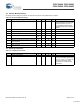
12.3.3 DC Operational Amplifier Specifications
The following tables list guaranteed maximum and minimum specifications for the voltage and temperature ranges: 4.75V to 5.25V
and -40°C ≤ T
A
≤ 85°C, or 3.0V to 3.6V and -40°C ≤ T
A
≤ 85°C, respectively. Typical parameters apply to 5V and 3.3V at 25°C and
are for design guidance only.
The Operational Amplifier is a component of both the Analog Continuous Time PSoC blocks and the Analog Switched Cap PSoC
blocks. The guaranteed specifications are measured in the Analog Continuous Time PSoC block. Typical parameters apply to 5V at
25°C and are for design guidance only.
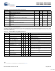
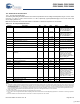
Table 12-6. 5V DC Operational Amplifier Specifications
Symbol Description Min Typ Max Unit Notes
V
OSOA
Input Offset Voltage (absolute value)
Power = Low, Opamp Bias = High
Power = Medium, Opamp Bias = High
Power = High, Opamp Bias = High
–1.6
1.3
1.2
10
8
7.5
mV
mV
mV
–
–
TCV
OSOA
Average Input Offset Voltage Drift – 7.0 35.0 μV/
o
C
I
EBOA
Input Leakage Current (Port 0 Analog Pins) – 200 – pA Gross tested to 1 μA.
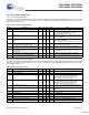
C
INOA
Input Capacitance (Port 0 Analog Pins) – 4.5 9.5 pF Package and pin dependent. Temp = 25
o
C.
V
CMOA
Common Mode Voltage Range. All Cases, except
highest.
Power = High, Opamp Bias = High
0.0 – Vdd
Vdd - 0.5
V
V
0.5 –
CMRR
OA
Common Mode Rejection Ratio 60 – – dB
G
OLOA
Open Loop Gain 80 – – dB
V
OHIGHO
A
High Output Voltage Swing (internal signals) Vdd - .01 – – V
V
OLOWOA
Low Output Voltage Swing (internal signals) – – 0.1 V
I
SOA
Supply Current (including associated AGND buffer)
Power = Low, Opamp Bias = Low
Power = Low, Opamp Bias = High
Power = Medium, Opamp Bias = Low
Power = Medium, Opamp Bias = High
Power = High, Opamp Bias = Low
Power = High, Opamp Bias = High
–
–
–
–
–
–
150
300
600
1200
2400
4600
200
400
800
1600
3200
6400
μA
μA
μA
μA
μA
μA
PSRR
OA
Supply Voltage Rejection Ratio 67 80 – dB Vss ≤ VIN ≤ (Vdd - 2.25) or
(Vdd - 1.25V) ≤ VIN ≤ Vdd.
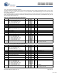
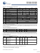
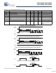
Table 12-7. 3.3V DC Operational Amplifier Specifications
Symbol Description Min Typ Max Unit Notes
V
OSOA
Input Offset Voltage (absolute value)
Power = Low, Opamp Bias = High
Power = Medium, Opamp Bias = High
High Power is 5 Volts Only
–
–
1.65
1.32
10
8
mV
mV
TCV
OSOA
Average Input Offset Voltage Drift – 7.0 35.0 μV/
o
C
I
EBOA
Input Leakage Current (Port 0 Analog Pins) – 200 – pA Gross tested to 1 μA.
C
INOA
Input Capacitance (Port 0 Analog Pins) – 4.5 9.5 pF Package and pin dependent. Temp = 25
o
C.
V
CMOA
Common Mode Voltage Range 0 – Vdd V
CMRR
OA
Common Mode Rejection Ratio 60 – – dB
G
OLOA
Open Loop Gain 80 – – dB
V
OHIGHO
A
High Output Voltage Swing (internal signals) Vdd - .01 – – V
V
OLOWOA
Low Output Voltage Swing (internal signals) – – .01 V
I
SOA
Supply Current (including associated AGND buffer)
Power = Low, Opamp Bias = Low
Power = Low, Opamp Bias = High
Power = Medium, Opamp Bias = Low
Power = Medium, Opamp Bias = High
Power = High, Opamp Bias = Low
Power = High, Opamp Bias = High
–
–
–
–
–
–
150
300
600
1200
2400
–
200
400
800
1600
3200
–
μA
μA
μA
μA
μA
Not Allowed
PSRR
OA
Supply Voltage Rejection Ratio 54 80 – dB Vss ≤ VIN ≤ (Vdd - 2.25) or
(Vdd - 1.25V) ≤ VIN ≤ Vdd
[+] Feedback