
User manual

CY8C29466, CY8C29566
CY8C29666, CY8C29866
Document Number: 38-12013 Rev. *M Page 25 of 47
12.3.6 DC Switch Mode Pump Specifications
The following table lists guaranteed maximum and minimum specifications for the voltage and temperature ranges: 4.75V to 5.25V
and -40°C ≤ T
A
≤ 85°C, or 3.0V to 3.6V and -40°C ≤ T
A
≤ 85°C, respectively. Typical parameters apply to 5V and 3.3V at 25°C and
are for design guidance only.
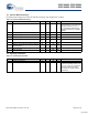
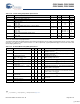
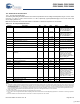
Table 12-10. 3.3V DC Analog Output Buffer Specifications
Symbol Description Min Typ Max Units
V
OSOB
Input Offset Voltage (Absolute Value) – 3 12 mV
TCV
OSOB
Average Input Offset Voltage Drift – +6 – μV/°C
V
CMOB
Common-Mode Input Voltage Range 0.5 - Vdd - 1.0 V
R
OUTOB
Output Resistance
Power = Low
Power = High
–
–
–
–
10
10
W
W
V
OHIGHOB
High Output Voltage Swing (Load = 1k ohms to Vdd/2)
Power = Low
Power = High
0.5 x Vdd
+ 1.0
0.5 x Vdd
+ 1.0
–
–
–
–
V
V
V
OLOWOB
Low Output Voltage Swing (Load = 1k ohms to Vdd/2)
Power = Low
Power = High
–
–
–
–
0.5 x Vdd
- 1.0
0.5 x Vdd
- 1.0
V
V
I
SOB
Supply Current Including Bias Cell (No Load)
Power = Low
Power = High –
0.8
2.0
1
5
mA
mA
PSRR
OB
Supply Voltage Rejection Ratio 60 64 – dB
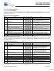
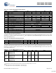
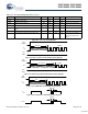
Table 12-11. DC Switch Mode Pump (SMP) Specifications
Symbol Description Min Typ Max Unit Notes
V
PUMP
5V 5V Output Voltage at Vdd from Pump 4.75 5.0 5.25 V Configuration of footnote.
[3]
Average, neglecting ripple. SMP trip
voltage is set to 5.0V.
V
PUMP
3V 3V Output Voltage at Vdd from Pump 3.00 3.25 3.60 V Configuration of footnote.
[3]
Average, neglecting ripple. SMP trip
voltage is set to 3.25V.
I
PUMP
Available Output Current
V
BAT
= 1.5V, V
PUMP
= 3.25V
V
BAT
= 1.8V, V
PUMP
= 5.0V
8
5
–
–
–
–
mA
mA
Configuration of footnote.
[3]
SMP trip voltage is set to 3.25V.
SMP trip voltage is set to 5.0V.
V
BAT
5V Input Voltage Range from Battery 1.8 – 5.0 V Configuration of footnote.
[3]
SMP trip voltage is set to 5.0V.
V
BAT
3V Input Voltage Range from Battery 1.0 – 3.3 V Configuration of footnote.
[3]
SMP trip voltage is set to 3.25V.
V
BATSTART
Minimum Input Voltage from Battery
to Start Pump
1.2 – – V Configuration of footnote.
[3]
0
o
C ≤ T
A
≤ 100. 1.25V at T
A
= -40
o
C.
ΔV
PUMP_Line
Line Regulation (over V
BAT
range) – 5 – %V
O
Configuration of footnote.
[3]
V
O
is the “Vdd Value for PUMP Trip”
specified by the VM[2:0] setting in the DC POR and LVD Speci-
fication, Table 3-15 on page 27.
ΔV
PUMP_Load
Load Regulation – 5 – %V
O
Configuration of footnote.
[3]
V
O
is the “Vdd Value for PUMP Trip”
specified by the VM[2:0] setting in the DC POR and LVD Speci-
fication, Table 3-15 on page 27.
ΔV
PUMP_Ripple
Output Voltage Ripple (depends on
capacitor/load)
– 100 – mVp
p
Configuration of footnote.
[3]
Load is 5 mA.
E
3
Efficiency 35 50 – % Configuration of footnote.
[3]
Load is 5 mA. SMP trip voltage is
set to 3.25V.
F
PUMP
Switching Frequency – 1.4 – MHz
DC
PUMP
Switching Duty Cycle – 50 – %
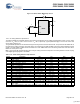
Note
3. L
1
= 2 μH inductor, C
1
= 10 μF capacitor, D
1
= Schottky diode. See Figure 12-3..
[+] Feedback