
User manual

CY8C29466, CY8C29566
CY8C29666, CY8C29866
Document Number: 38-12013 Rev. *M Page 26 of 47
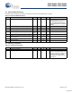
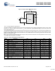
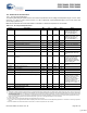
Figure 12-3. Basic Switch Mode Pump Circuit
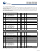
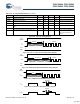
12.3.7 DC Analog Reference Specifications
The following tables list guaranteed maximum and minimum specifications for the voltage and temperature ranges: 4.75V to 5.25V
and -40°C ≤ T
A
≤ 85°C, or 3.0V to 3.6V and -40°C ≤ T
A
≤ 85°C, respectively. Typical parameters apply to 5V and 3.3V at 25°C and
are for design guidance only.
The guaranteed specifications are measured through the Analog Continuous Time PSoC blocks. The power levels for AGND refer to
the power of the Analog Continuous Time PSoC block. The power levels for RefHi and RefLo refer to the Analog Reference Control
register. The limits stated for AGND include the offset error of the AGND buffer local to the Analog Continuous Time PSoC block.
Reference control power is high.
Note Avoid using P2[4] for digital signaling when using an analog resource that depends on the Analog Reference. Some coupling
of the digital signal may appear on the AGND.
Battery
C1
D1
+
PSoC
Vdd
Vss
SMP
V
BAT
V
PUMP
L
1
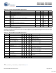
Table 12-12. 5V DC Analog Reference Specifications
Symbol Description Min Typ Max Unit
V
BG5
Bandgap Voltage Reference 5V 1.28 1.30 1.32 V
– AGND = Vdd/2
[4]
Vdd/2 - 0.02 Vdd/2 Vdd/2 + 0.02 V
– AGND = 2 x BandGap
[4]
2.52 2.60 2.72 V
– AGND = P2[4] (P2[4] = Vdd/2)
[4]
P2[4] - 0.013 P2[4] P2[4] + 0.013 V
– AGND = BandGap
[4]
1.27 1.3 1.34 V
– AGND = 1.6 x BandGap
[4]
2.03 2.08 2.13 V
– AGND Block to Block Variation (AGND = Vdd/2)
[4]
-0.034 0.000 0.034 V
– RefHi = Vdd/2 + BandGap Vdd/2 + 1.21 Vdd/2 + 1.3 Vdd/2 + 1.382 V
– RefHi = 3 x BandGap 3.75 3.9 4.05 V
– RefHi = 2 x BandGap + P2[6] (P2[6] = 1.3V) P2[6] + 2.478 P2[6] + 2.6 P2[6] + 2.722 V
– RefHi = P2[4] + BandGap (P2[4] = Vdd/2) P2[4] + 1.218 P2[4] + 1.3 P2[4] + 1.382 V
– RefHi = P2[4] + P2[6] (P2[4] = Vdd/2, P2[6] = 1.3V) P2[4] + P2[6] - 0.058 P2[4] + P2[6] P2[4] + P2[6] + 0.058 V
– RefHi = 2 x BandGap 2.50 2.60 2.70 V
– RefHi = 3.2 x BandGap 4.02 4.16 4.29 V
– RefLo = BandGap BG - 0.082 BG + 0.023 BG + 0.129 V
– RefLo = 2 x BandGap - P2[6] (P2[6] = 1.3V) 2 x BG - P2[6] - 0.084 2 x BG - P2[6] + 0.025 2 x BG - P2[6] + 0.134 V
– RefLo = P2[4] – BandGap
(P2[4] = Vdd/2)
P2[4] - BG - 0.056 P2[4] - BG + 0.026 P2[4] - BG + 0.107 V
– RefLo = P2[4]-P2[6] (P2[4] = Vdd/2, P2[6] = 1.3V) P2[4] - P2[6] - 0.057 P2[4] - P2[6] + 0.026 P2[4] - P2[6] + 0.110 V
[+] Feedback