
User manual

CY8C29466, CY8C29566
CY8C29666, CY8C29866
Document Number: 38-12013 Rev. *M Page 27 of 47
12.3.8 DC Analog PSoC Block Specifications
The following table lists guaranteed maximum and minimum specifications for the voltage and temperature ranges: 4.75V to 5.25V
and -40°C ≤ T
A
≤ 85°C, or 3.0V to 3.6V and -40°C ≤ T
A
≤ 85°C, respectively. Typical parameters apply to 5V and 3.3V at 25°C and
are for design guidance only.
12.3.9 DC POR, SMP, and LVD Specifications
The following table lists guaranteed maximum and minimum specifications for the voltage and temperature ranges: 4.75V to 5.25V
and -40°C ≤ T
A
≤ 85°C, or 3.0V to 3.6V and -40°C ≤ T
A
≤ 85°C, respectively. Typical parameters apply to 5V and 3.3V at 25°C and
are for design guidance only.
Note
4. AGND tolerance includes the offsets of the local buffer in the PSoC block. Bandgap voltage is 1.3V ± 0.02V.
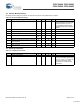
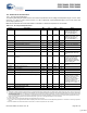
Table 12-13. 3.3V DC Analog Reference Specifications
Symbol Description Min Typ Max Unit
V
BG33
Bandgap Voltage Reference 3.3V 1.28 1.30 1.32
V
– AGND = Vdd/2
[4]
Vdd/2 - 0.02 Vdd/2 Vdd/2 + 0.02
V
– AGND = 2 x BandGap
[4]
Not Allowed
– AGND = P2[4] (P2[4] = Vdd/2) P2[4] - 0.009 P2[4] P2[4] + 0.009
V
– AGND = BandGap
[4]
1.27 1.30 1.34
V
– AGND = 1.6 x BandGap
[4]
2.03 2.08 2.13
V
– AGND Block to Block Variation (AGND = Vdd/2)
[4]
-0.034 0.000 0.034
mV
– RefHi = Vdd/2 + BandGap Not Allowed
– RefHi = 3 x BandGap Not Allowed
– RefHi = 2 x BandGap + P2[6] (P2[6] = 0.5V) Not Allowed
– RefHi = P2[4] + BandGap (P2[4] = Vdd/2) Not Allowed
– RefHi = P2[4] + P2[6] (P2[4] = Vdd/2, P2[6] = 0.5V) P2[4] + P2[6] - 0.042 P2[4] + P2[6] P2[4] + P2[6] + 0.042
V
– RefHi = 2 x BandGap 2.50 2.60 2.70
V
– RefHi = 3.2 x BandGap Not Allowed
– RefLo = Vdd/2 - BandGap
Not Allowed
– RefLo = BandGap
Not Allowed
– RefLo = 2 x BandGap - P2[6] (P2[6] = 0.5V)
Not Allowed
– RefLo = P2[4] – BandGap (P2[4] = Vdd/2)
Not Allowed
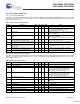
Table 12-14. DC Analog PSoC Block Specifications
Symbol Description Min Typ Max Unit Notes
R
CT
Resistor Unit Value (Continuous Time) – 12.2 – kΩ
C
SC
Capacitor Unit Value (Switch Cap) – 80 – fF
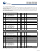
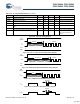
Table 12-15. DC POR, SMP, and LVD Specifications
Symbol Description Min Typ Max Units Notes
V
PPOR0R
V
PPOR1R
V
PPOR2R
Vdd Value for PPOR Trip (positive ramp)
PORLEV[1:0] = 00b
PORLEV[1:0] = 01b
PORLEV[1:0] = 10b
–
2.91
4.39
4.55
–
V
V
V
V
PPOR0
V
PPOR1
V
PPOR2
Vdd Value for PPOR Trip (negative ramp)
PORLEV[1:0] = 00b
PORLEV[1:0] = 01b
PORLEV[1:0] = 10b
–
2.82
4.39
4.55
–
V
V
V
V
PH0
V
PH1
V
PH2
PPOR Hysteresis
PORLEV[1:0] = 00b
PORLEV[1:0] = 01b
PORLEV[1:0] = 10b
–
–
–
92
0
0
–
–
–
mV
mV
mV
Notes
5. Always greater than 50 mV above PPOR (PORLEV = 00) for falling supply.
6. Always greater than 50 mV above PPOR (PORLEV = 10) for falling supply.
[+] Feedback