
User manual

CY8C29466, CY8C29566
CY8C29666, CY8C29866
Document Number: 38-12013 Rev. *M Page 3 of 47
4. PSoC Functional Overview
The PSoC family consists of many Programmable
System-on-Chip Controller devices. These devices are designed
to replace multiple traditional MCU-based system components
with one, low cost single-chip programmable device. PSoC
devices include configurable blocks of analog and digital logic,
as well as programmable interconnects. This architecture allows
the user to create customized peripheral configurations that
match the requirements of each individual application.
Additionally, a fast CPU, Flash program memory, SRAM data
memory, and configurable I/O are included in a range of conve-
nient pinouts and packages.
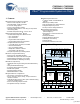
The PSoC architecture, as illustrated on the left, is comprised of
four main areas: PSoC Core, Digital System, Analog System,
and System Resources. Configurable global busing allows all
the device resources to be combined into a complete custom
system. The PSoC CY8C29x66 family can have up to five I/O
ports that connect to the global digital and analog interconnects,
providing access to 8 digital blocks and 12 analog blocks.
4.1 PSoC Core
The PSoC Core is a powerful engine that supports a rich feature
set. The core includes a CPU, memory, clocks, and configurable
GPIO (General Purpose I/O).
The M8C CPU core is a powerful processor with speeds up to 24
MHz, providing a four MIPS 8-bit Harvard architecture micropro-
cessor. The CPU uses an interrupt controller with 17 vectors, to
simplify programming of real time embedded events. Program
execution is timed and protected using the included Sleep and
Watch Dog Timers (WDT).
Memory encompasses 16K of Flash for program storage, 256
bytes of SRAM for data storage, and up to 2K of EEPROM
emulated using the Flash. Program Flash utilizes four protection
levels on blocks of 64 bytes, allowing customized software IP
protection.
The PSoC device incorporates flexible internal clock generators,
including a 24 MHz IMO (internal main oscillator) accurate to
2.5% over temperature and voltage. The 24 MHz IMO can also
be doubled to 48 MHz for use by the digital system. A low power
32 kHz ILO (internal low speed oscillator) is provided for the
Sleep timer and WDT. If crystal accuracy is desired, the ECO
(32.768 kHz external crystal oscillator) is available for use as a
Real Time Clock (RTC) and can optionally generate a
crystal-accurate 24 MHz system clock using a PLL. The clocks,
together with programmable clock dividers (as a System
Resource), provide the flexibility to integrate almost any timing
requirement into the PSoC device.
PSoC GPIOs provide connection to the CPU, digital and analog
resources of the device. Each pin’s drive mode may be selected
from eight options, allowing great flexibility in external inter-
facing. Every pin also has the capability to generate a system
interrupt on high level, low level, and change from last read.
4.2 Digital System
The Digital System is composed of 8 digital PSoC blocks. Each
block is an 8-bit resource that can be used alone or combined
with other blocks to form 8, 16, 24, and 32-bit peripherals, which
are called user module references.
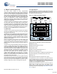
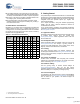
Figure 4-1. Digital System Block Diagram
Digital peripheral configurations include those listed below.
■ PWMs (8 to 32 bit)
■ PWMs with Dead band (8 to 32 bit)
■ Counters (8 to 32 bit)
■ Timers (8 to 32 bit)
■ UART 8 bit with selectable parity (up to 2)
■ SPI slave and master (up to 2)
■ I
2
C slave and multi-master (1 available as a System Resource)
■ Cyclical Redundancy Checker/Generator (8 to 32 bit)
■ IrDA (up to 2)
■ Pseudo Random Sequence Generators (8 to 32 bit)
The digital blocks can be connected to any GPIO through a
series of global buses that can route any signal to any pin. The
buses also allow for signal multiplexing and for performing logic
operations. This configurability frees your designs from the
constraints of a fixed peripheral controller.
Digital blocks are provided in rows of four, where the number of
blocks varies by PSoC device family. This allows you the
optimum choice of system resources for your application. Family
resources are shown in the table titled “PSoC Device Character-
istics” on page 5.
DIGITAL SYSTEM
To System Bus
D
i
g
i
t
a
l
C
l
o
c
k
s
F
r
o
m
C
o
r
e
Digital PSoC Block Array
To Analog
System
8
Row Input
Configuration
Row Output
Configuration
88
8
Row 1
DBB10 DBB11 DCB12 DCB13
Row Input
Configuration
4
4
Row Output
Configuration
Row 0
DBB00 DBB01 DCB02 DCB03
4
4
GIE[7:0]
GIO[7:0]
GOE[7:0]
GOO[7:0]
Global Digital
Interconnect
Por t 4
Por t 3
Por t 2
Por t 1
Por t 0
Po r t 5
[+] Feedback