
User manual


CY8CKIT-049-4xxx PSoC® 4 Prototyping Kit Guide, Doc. #: 001-90711 Rev. *G 31
Hardware
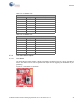
4.3.3.2 Functionality of J3 and J5 Headers (PSoC 4 to USB-Serial)
Both the USB-Serial and the PSoC 4 prototyping boards each contain a 1×4-pin header. This header
provides a physical connection between the two devices. Specifically, the connection includes the
UART (RX and TX), VDD, and GND connections between the two devices. When the boards are
separated, this physical connection is broken.
Figure 4-5. J3 and J5 Headers
Table 4-2. J2 Header Pin Details
PSoC 4 GPIO Header (J2)
Pin Signal Description
J2_01 VDD Power
J2_02 GND Ground
J2_03 RESET Reset
J2_04 P3.3 GPIO/SWDCLK
J2_05 P3.2 GPIO/SWDIO
J2_06 P3.7 GPIO
J2_07 P3.6 GPIO
J2_08 P3.5 GPIO
J2_09 P3.4 GPIO
J2_10 P3.3 GPIO/SWDCLK
J2_11 P3.2 GPIO/SWDIO
J2_12 P3.1 GPIO
J2_13 P3.0 GPIO
J2_14 P2.7 GPIO
J2_15 P2.6 GPIO
J2_16 P2.5 GPIO
J2_17 P2.4 GPIO
J2_18 P2.3 GPIO
J2_19 P2.2 GPIO
J2_20 P2.1 GPIO
J2_21 P2.0 GPIO
J2_22 GND Ground