CY8CKIT-050 PSoC® 5LP Development Kit Guide Doc. # 001-65816 Rev. *E Cypress Semiconductor 198 Champion Court San Jose, CA 95134-1709 Phone (USA): 800.858.1810 Phone (Intnl): 408.943.2600 http://www.cypress.
Copyrights Copyrights © Cypress Semiconductor Corporation, 2011-2012. The information contained herein is subject to change without notice. Cypress Semiconductor Corporation assumes no responsibility for the use of any circuitry other than circuitry embodied in a Cypress product. Nor does it convey or imply any license under patent or other rights.
Contents 1. Introduction 1.1 1.2 1.3 1.4 1.5 Kit Contents .................................................................................................................5 PSoC Creator ..............................................................................................................5 Additional Learning Resources....................................................................................6 1.3.1 Beginner Resources........................................................................
Contents 4.2.8 4.2.9 4.2.10 4.2.11 RS-232 Interface............................................................................................ 29 Prototyping Area ............................................................................................ 29 Character LCD ............................................................................................... 30 CapSense Sensors ........................................................................................ 31 5. Code Examples 5.1 5.
1. Introduction Thank you for your interest in the CY8CKIT-050 PSoC® 5 Development Kit. This kit allows you to develop precision analog and low-power designs using PSoC 5LP. You can design your own projects with PSoC Creator™ or alter the sample projects provided with this kit. The CY8CKIT-050 PSoC 5LP Development Kit is based on the PSoC 5LP family of devices. PSoC 5LP is a Programmable System-on-Chip™ platform for 8-bit, 16-bit, and 32-bit applications.
Introduction 1.3 Additional Learning Resources Visit http://www.cypress.com/go/psoc5 for additional learning resources in the form of datasheets, technical reference manual, and application notes. 1.3.1 Beginner Resources AN77759 - Getting Started with PSoC 5 PSoC Creator Training 1.3.
Introduction The Find Example project has various filters that help you locate the most relevant project you are looking for. PSoC Creator provides several Starter Designs. These designs highlight features that are unique to PSoC devices. They allow you to create a design with various components and code is also provided, instead of creating a new empty design. To use a starter design for your project, navigate to File->New->Project and select the design required.
Introduction The example projects and starter designs are designed for CY8CKIT-001 PSoC Development Kit. However, these projects can be converted for use with CY8CKIT-030 PSoC 3 Development Kit or CY8CKIT-050 PSoC 5 Development Kit by following the procedure in the knowledge base article Migrating project from CY8CKIT-001 to CY8CKIT-030 or CY8CKIT-050. Apart from the example projects and starter designs that are available within PSoC Creator, Cypress continuously strives to provide the best support.
Introduction 1.4 Document History Revision 1.5 PDF Creation Date Origin of Change Description of Change ** 03/01/2011 PVKV Initial version of kit guide *A 04/28/2011 RKAD Updated Schematic *B 12/15/2011 RKAD Added sections 4.2.1.4 and 4.2.1.5. Added Pin Assignment table in the Appendix. Updated bill of materials. Content updates throughout the document *C 05/15/2012 SASH Updated the Additional Resources section *D 06/18/2012 SASH Updated CD Installation on page 11.
Introduction 10 CY8CKIT-050 PSoC® 5LP Development Kit Guide, Doc. # 001-65816 Rev.
2. 2.1 Getting Started Introduction This chapter describes how to install and configure the PSoC 5LP Development Kit. Chapter 3 describes the kit operation. It explains how to program a PSoC 5LP device with PSoC Programmer and use the kit with the help of a code example. To reprogram the PSoC device with PSoC Creator, see the CD installation instructions for PSoC Creator. Chapter 4 details the hardware operation. Chapter 5 provides instructions to create a simple code example.
Getting Started After the installation is complete, the kit contents are available at the following location: :\PSoC 5LP Development Kit\ 2.3 Install Hardware No hardware installation is required for this kit. 2.4 Install Software When installing the PSoC 5LP Development Kit, the installer checks if your system has the required software. These include PSoC Creator, PSoC Programmer, Windows Installer, .NET, Acrobat Reader, and KEIL Complier.
3. Kit Operation The code examples in the PSoC 5LP Development Kit help you develop applications using the PSoC 5LP family of devices. The kit is designed to develop precision analog applications using PSoC 5LP. The board also has hooks to enable low-power measurements for low-power application development and evaluation. 3.1 Programming PSoC 5LP Device The default programming interface for the board is a USB-based on-board programming interface.
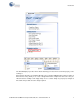
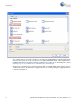
Kit Operation Figure 3-2. Connect MiniProg With the MiniProg3, programming is similar to the on-board programmer; however, the setup enumerates as a MiniProg3. Note Sometimes pop-up window will come as shown in figure below. 14 CY8CKIT-050 PSoC® 5LP Development Kit Guide, Doc. # 001-65816 Rev.
Kit Operation Then click on Port acquire, you will get following window. Then click on connect to start programming. CY8CKIT-050 PSoC® 5LP Development Kit Guide, Doc. # 001-65816 Rev.
Kit Operation 16 CY8CKIT-050 PSoC® 5LP Development Kit Guide, Doc. # 001-65816 Rev.
4. 4.
Hardware Figure 4-1. PSoC 5LP Development Kit Details Communication USB Power Adapter Boost Converter 9-V Battery Input 10-Pin JTAG/SWD/SWO Debug and Prog Header On-board Programming USB 10-Pin MiniTrace Connector 32-kHz Crystal 24-MHz Crystal Port D (CapSense/ Miscellaneous Port) Port E (Analog Port) Reset Button Variable Resistor/ Potentiometer CapSense RS-232 Interface Prototyping Area Character LCD Interface 4.2 Functional Description 4.2.
Hardware The board power domain has five rails: ■ Vin rail: This is where the input of the on-board regulators are connected. This domain is powered through protection diodes. ■ 5-V rail: This is the output of the 5-V regulator U2. The rail is a fixed 5-V output regardless of jumper settings. The voltage in this rail can be less than 5 V only when the board is powered by the USB. This 5-V rail powers the circuits that require fixed 5-V supply. ■ 3.3-V rail: This is the output of the 3.
Hardware Two jumpers govern the power rails on the board. J10 is responsible for the selection of Vddd (digital power) and J11 selects the VADJ of Vdda (analog power). The jumper settings for each power scheme are as follows. Powering Scheme Jumper Settings Vdda = 5 V, Vddd = 5 V J10 in 5 V setting and J11 in 5 V setting. Vdda = 3.3 V, Vddd = 3.3 V J10 in 3.3 V setting and J11 in 3.3 V setting. Vdda = 5 V, Vddd = 3.3 V J10 in 3.3 V setting and J11 in 5 V setting. Vdda = 3.
Hardware The board provides the ability to measure analog and digital power separately. To measure power at a single point, rather than at analog and digital separately, remove the resistor R23 to disconnect the analog regulator from powering the Vdda and short Vdda and Vddd through R30. Now, the net power can be measured at the J10 jumper similar to the digital power measurement. To switch repeatedly between R23 and R30, moving around the zero-ohm resistors can be discomforting.
Hardware Figure 4-4. On-board Programming Interface When the USB programming is plugged into the PC, it enumerates as DVKProg5 and you can use the normal programming interface from PSoC Creator to program this board through the on-board programmer. A zero-ohm resistor R9 is provided on the board to disconnect power to the on-board programmer. 4.2.2.2 JTAG/SWD Programming Apart from the on-board programming interface, the board also provides the option of using the MiniProg3.
Hardware The JTAG/SWD programming using J3 requires the programmer, which can be purchased from http://www.cypress.com/go/CY8CKIT-002. Note While using MiniProg3, only Reset mode is supported with this Kit. 4.2.3 USB Communication The board has a USB communications interface that uses the connector, as shown in Figure 4-6. The USB connector connects to the D+ and D– lines on the PSoC to enable development of USB applications using the board.
Hardware Figure 4-7. Boost Converter 4.2.5 32-kHz and 24-MHz Crystal PSoC 5LP has an on-chip real time clock (RTC), which can function in sleep. This requires an external 32-kHz crystal, which is provided on the board to facilitate RTC-based designs. The PSoC 5LP also has an external MHz crystal option in applications where the IMO tolerance is not satisfactory. In these applications, the board has a 24-MHz crystal to provide an accurate main oscillator. 4.2.
Hardware Figure 4-8. Schematic for Protection Circuit on 5-V Power Line Figure 4-9. Schematic for Protection Circuit on 3.3-V Power Line 4.2.6.1 Functional Description of Circuit The protection circuit will protect from a maximum over-voltage or reverse-voltage of 12 Volts. The cut-off voltage on the 5-V line is 5.7 V and on the 3.3-V line is 3.6 V.
Hardware If you intend to use the regulator power supply from the board to power the external modules, both the P-MOS Q4 and Q5 will always be on, allowing the flow of current with a maximum of 22 mV drop across the circuit when the current consumed by the external module is 150 mA. Note The working of protection circuit on the 3.3-V line and 5-V line is as described above. For the purpose of explanation, the annotation of 3.3-V protection circuitry (Figure 4-9) is used. 4.2.
Hardware Figure 4-10. Port D CY8CKIT-050 PSoC® 5LP Development Kit Guide, Doc. # 001-65816 Rev.
Hardware 4.2.7.2 Port E This is the analog port on this kit and has special layout considerations. It also brings out all analog resources such as dedicated opamps to a single connect. Therefore, this port is ideal for precision analog design development. This port is functionally compatible to port A of the PSoC Development Kit and it is easy to port an application developed on port A. This port has two types of grounds, CGND1 and CGND2.
Hardware 4.2.8 RS-232 Interface The board has an RS-232 transceiver for designs using RS-232 (UART). The RS-232 section power can be disconnected through a single resistor R58. This is useful for low-power designs. Figure 4-12. RS-232 Interface 4.2.9 Prototyping Area The prototyping area on the board has two complete ports of the device for simple custom circuit development. The ports in the area are port 0 and port 3, which bring out the four dedicated opamp pins on the device.
Hardware Figure 4-13. Prototyping Area This area also comprises of a potentiometer to be used for analog system development work. The potentiometer connects from Vdda, which is a noise free supply and is hence capable of being used for low noise analog applications. The potentiometer output is available on P6[5] and VR on header P6 in the prototyping area. 4.2.10 Character LCD The kit has a character LCD module, which goes into the character LCD header, P8. The LCD runs on a 3.
Hardware Figure 4-15. LCD Connected on P8 Connector 4.2.11 CapSense Sensors The board layout considers the special requirements for CapSense. It has two CapSense buttons and a 5-element CapSense slider. The CapSense buttons are connected to pins P5[6] and P5[5]. The slider elements are connected to pins P5[0:4]. The Cmod (modulation capacitor) is connected to pin P6[4] and an optional Rb (bleeder resistor) is available on P15[4]. CY8CKIT-050 PSoC® 5LP Development Kit Guide, Doc. # 001-65816 Rev.
Hardware Figure 4-16. CapSense Sensors 32 CY8CKIT-050 PSoC® 5LP Development Kit Guide, Doc. # 001-65816 Rev.
5. Code Examples To access code examples described in this section, open the PSoC Creator Start Page. For additional code examples, visit http://www.cypress.com. Figure 5-1. PSoC Creator Start Page Follow these steps to open and program code examples: 1. Click on a code example from Examples and Kits on the PSoC Creator Start Page. 2. Create a folder in the desired location and click OK. 3. The project opens in PSoC Creator and is saved to that folder. 4. Build the code example to generate the hex file.
Code Examples 5.1 Project: VoltageDisplay_SAR_ADC 5.1.1 Project Description This example code measures an analog voltage controlled by the potentiometer. The code uses the internal SAR ADC configured for a 12-bit operation; the ADC range is 0 to Vdda. The results are displayed on the character LCD. Note The PSoC 5LP Development Kit is factory-programmed with this example. 5.1.2 Hardware Connections The example requires the character LCD on P8.
Code Examples 5.1.4 ■ Range is set to Vssa to Vdda in single-ended mode because the potentiometer output is a single ended signal that can go from 0 to Vdda. Therefore, at 12-bit resolution, the ADC will resolve in steps of Vdda/212. ■ Voltage Reference should be set to Vdda/2 supply voltage when input range is set to ‘Vssa to Vdda’. It is set to 1.65 V here, because by default Vdda jumper setting on the board is set to 3.3 V. If J11 is changed to select 5 V, then this parameter should be changed to 2.
Code Examples 5.2.2 Hardware Connections The example requires the character LCD on P8. Because it uses the potentiometer, the jumper POT_PWR should be in place. This connects the potentiometer to the Vdda. Move jumper J10 and J11 to position 2-3, this will set Vdda to 5 V. 5.2.3 Del-Sig ADC Configuration To view or configure the Delsig ADC component, double-click the component in the TopDesign.cysch file. Figure 5-4.
Code Examples ADC. To set Vdda to 5 V, in the VoltageDisplay_DelSigADC.cydwr window of PSoC Creator, click on the System tab, go to Operating Conditions options. Set Vdda to 5 V. 5.2.4 Verify Output Build and program the code example, and reset the device. The LCD shows the voltage reading corresponding to the voltage on the potentiometer. Figure 5-5 demonstrates the functionality. When you turn the potentiometer, the voltage value changes.
Code Examples 5.3 Project: IntensityLED 5.3.1 Project Description This example code uses a pulse-width modulator (PWM) to illuminate an LED. When the pulse width of the PWM varies, the LED brightness changes. By continuously varying the pulse width of the PWM, the example code makes an LED go from low brightness to a high brightness and back. 5.3.2 Hardware Connections No hardware connections are required for this project, because all the connections are hard-wired to specific pins on the board. 5.3.
Code Examples 5.4.3 Verify Output In normal operation, the project displays the time starting from 00:00:00 when SW2 is pressed. Normal mode is indicated by LED3 in ON state. When you press the SW2 button again, the device is put to sleep. Sleep mode is indicated by LED3 in OFF state. If an ammeter is connected to measure the system current (refer Low-Power Functionality on page 20 for details), a system current of less than 2 µA is displayed.
Code Examples 5.5.2 Hardware Connections This project uses the LCD for display; therefore, ensure that it is plugged into the port. No specific hardware connections are required for this project because all connections are hard-wired on the board. 5.5.3 Verify Output Build and program the code example, and reset the device. The LCD displays the status of the two buttons as On/Off. The LCD also shows the slider touch position as a percentage.
Code Examples Figure 5-10. CapSense Button 5.6 Project: ADC_DAC 5.6.1 Project Description This project demonstrates sine wave generation by using an 8-bit DAC and DMA. The sine wave period is based on the current value of the ADC value of the potentiometer. The firmware reads the voltage output by the board potentiometer and displays the raw counts on the board character LCD display. An 8-bit DAC outputs a table generated sine wave to an LED using DMA at a frequency proportional to the ADC count. 5.6.
Code Examples Figure 5-11. ADC Output 42 CY8CKIT-050 PSoC® 5LP Development Kit Guide, Doc. # 001-65816 Rev.
Schematic Power Supply NO LOAD TP4 RED V5.0 5.0V/1A LDO U2 3 3216 R24 AP1117D50G TO-252 VIN + 2 VOUT 2 C143216 + D-64 2 9V Battery Terminals 10 uFd 16v GND 1 TP3 RED NO LOAD VSSD GND V3.3 R26 ZERO V5.0 0805 SS12-E3/61T GND LM1117MPX-3.3 2 VOUT GND 4 TAB 3216 U4 + C15 10 uFd 16v VDDA GND + C5 GND GND1 GND2 nSHDN 4 Byp VDDA GND VSSD 1 1 VSSB ZERO NO LOAD VSSA VSSD 1 NO LOAD 1 VDDD R11 1K 3 2 1 0805 0805 1 2 3 VSSA LED Green D5 R57 J38 V5.0 V3.
CY8CKIT-050 PSoC® 5LP Development Kit Guide, Doc. # 001-65816 Rev.
C7 0402 C18 0402 0.1 uFd C12 0402 0.1 uFd PLACE ONE CAP PER EACH VCC ON U5. 0.1 uFd 2 VDDD 13 TV-20R TV2 1 TP2 54 1 44 29 30 31 NO LOAD 3V3_FX12P GND SCL 8-SOIC R6 2.2K R5 2.2K 1 2 WAKEUP# CTL0/FLAGA CTL1/FLAGB CTL2/FLAGC 15 16 SCL SDA 0.
GND CGND1 Use Separate Track for CGND1 to GND P1 P3[6] P3[4] P3[2] P3[0] J23 1 1 P0[6] P0[4] P0[2] P0[0] NO LOAD J20 1 1 P4[6] P4[4] P4[2] P4[0] NO LOAD J17 1 1 NO LOAD J13 1 P12[2] SCL P12[0] 1 V5.
CY8CKIT-050 PSoC® 5LP Development Kit Guide, Doc. # 001-65816 Rev.
CY8CKIT-050 PSoC® 5LP Development Kit Guide, Doc. # 001-65816 Rev.
A.2 Board Layout A.2.1 PDC-09356 Top CY8CKIT-050 PSoC® 5LP Development Kit Guide, Doc. # 001-65816 Rev.
A.2.2 50 PDC-09356 Power CY8CKIT-050 PSoC® 5LP Development Kit Guide, Doc. # 001-65816 Rev.
A.2.3 PDC-09356 Ground CY8CKIT-050 PSoC® 5LP Development Kit Guide, Doc. # 001-65816 Rev.
A.2.4 52 PDC-09356 Bottom CY8CKIT-050 PSoC® 5LP Development Kit Guide, Doc. # 001-65816 Rev.
A.3 Bill of Materials (BOM) Item Qty Reference Value Description Manufacturer Manufacturer Part No.
Item Qty Reference Value Description TEST POINT PC MINI .040"D Black Keystone Electronics Manufacturer Part No. 22 5 23 4 LED1,LED2,LED3 LED Red ,LED4 LED RED CLEAR 0805 SMD Rohm SemiconSML-210LTT86 ductor 24 1 L1 22 uH INDUCTOR SHIELD PWR 22UH 7032 TDK Corporation 25 2 P1,P2 20x2 RECP RA CONN FMALE 40POS DL .100 Sullins ElectronPPPC202LJBN-RC R/A GOLD ics Corp. 26 1 P7 DB9 FEMALE CONN DB9 FMALE VERT PRESSFIT SLD Norcomp Inc.
Item Qty Reference Value Description Manufacturer Manufacturer Part No. 44 1 R56 POT 10K POT 10K OHM 1/8W CARB VERTICAL CTS Electrocomponents 296UD103B1N 45 1 R58 10E RES 10 OHM 1/8W 5% 0805 SMD Stackpole Electronics Inc RMCF 1/10 10 5% R 46 1 R68 100 ohm RES 100 OHM 1/16W 5% 0603 Panasonic SMD ECG ERJ-3GEYJ101V 47 1 R69 10K RES 10K OHM 1/16W 5% 0603 Panasonic SMD ECG ERJ-3GEYJ103V 48 3 SW1,SW2,SW3 SW PUSHBUTTON LT SWITCH 6MM 160GF H=2.
Item Qty Reference Value Description Manufacturer Manufacturer Part No. 68 1 P5 4x1 RECP CONN RECEPT 4POS .100 VERT GOLD 69 1 J31, J32, J29, J34 4x1 RECP CONN RECEPT 4POS .100 VERT GOLD 3M 929850-01-04-RA CAP CERAMIC 1.0UF 25V X5R 0603 10% Taiyo Yuden TMK107BJ105KA-T 3M 929850-01-04-RA No Load Components 70 1 C24 1.0 uFd 71 11 J5,J6,J12,J14,J18 ,J22,J25,TP3,TP4 RED ,J16,J39 TEST POINT PC MINI .040"D RED Keystone Electronics 5000 72 2 J7,J36 BLACK TEST POINT PC MINI .
Item Qty Reference Value Description Manufacturer Manufacturer Part No. 88 1 J30 Install jumper across pins 1 and 2 Rectangular Connectors MINI JUMPER GF 13.5 CLOSE TYPE BLACK Kobiconn 151-8030-E 89 2 J10, J11 Install jumper across pins 1 and 2 Rectangular Connectors MINI JUMPER GF 13.5 CLOSE TYPE BLACK Kobiconn 151-8030-E 90 2 J43,J44 Install jumper across pins 1 and 2 Rectangular Connectors MINI JUMPER GF 13.
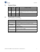
A.4 Port Port 0 Pin Assignment Table Pin Pin Name 71 P0[0] Connected to Pin 18 on Port E 72 P0[1] Connected to Pin 17 on Port E 73 P0[2] 74 P0[3] 76 P0[4] 77 P0[5] Connected to Pin 13 on Port E 78 P0[6] Connected to Pin 12 on Port E 79 P0[7] Connected to Pin 11 on Port E P1[0] Connected to 3 points: 1. Connected to Pin 2 on programming header J3 2. Connected to Pin 45 on U5 3. Connected to Pin 8 (SWDIO) on Port D 21 P1[1] Connected to 3 points: 1.
Port Pin Pin Name 95 P2[0] Connected to 2 points: 1. Connected to LCD module 2. Connected to Pin 18 on Port D 96 P2[1] Connected to 2 points: 1. Connected to LCD module 2. Connected to Pin 17 on Port D 97 P2[2] Connected to 2 points: 1. Connected to LCD module 2. Connected to Pin 16 on Port D P2[3] Connected to 3 points: 1. Connected to Pin 2 on trace header J40 2. Connected to LCD module 3. Connected to Pin 15 on Port D P2[4] Connected to 3 points: 1.
Port Port 5 Port 6 Port 12 60 Pin Pin Name Description 16 P5[0] Connected to 2 points: 1. Connected to CapSense slider segment 2. Connected to Pin 28 on Port D 17 P5[1] Connected to 2 points: 1. Connected to CapSense slider segment 2. Connected to Pin 27 on Port D 18 P5[2] Connected to 2 points: 1. Connected to CapSense slider segment 2. Connected to Pin 26 on Port D 19 P5[3] Connected to 2 points: 1. Connected to CapSense slider segment 2.
Port Port 15 Other Pins Pin Pin Name 42 P15[0] Description Connected to 24MHz Crystal 43 P15[1] Connected to 24MHz Crystal 55 P15[2] Connected to 32KHz Crystal 56 P15[3] Connected to 32KHz Crystal 93 P15[4] Connected to Rbleed resistor 94 P15[5] Connected to SW3 push button 35 P15[6] Connected to USB D+ 36 P15[7] Connected to USB D- 13 Vbat Connected to Vbat 12 Vboost Connected to Vboost 63 VCCa Connected to VCCa 39 VCCd Connected to VCCd 86 VCCd Connected to VCCd
CY8CKIT-050 PSoC® 5LP Development Kit Guide, Doc. # 001-65816 Rev.