
User manual


CY8CKIT-050 PSoC® 5LP Development Kit Guide, Doc. # 001-65816 Rev. *E 17
4. Hardware
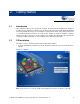
4.1 System Block Diagram
The PSoC 5LP Development Kit has the following sections:
■ Power supply system
■ Programming interface
■ USB communications
■ Boost convertor
■ PSoC 5LP and related circuitry
■ 32-kHz crystal
■ 24-MHz crystal
■ Port E (analog performance port) and port D (CapSense
®
or generic port)
■ RS-232 communications interface
■ Prototyping area
■ Character LCD interface
■ CapSense buttons and sliders
Note P0[2] is connected to SAR bypass capacitor C40 that can be selected by shorting jumper J43
and P0[4] is connected to SAR bypass capacitor C55 that can be selected by shorting jumper J44.