
User manual


58 CY8CKIT-050 PSoC® 5LP Development Kit Guide, Doc. # 001-65816 Rev. *E
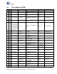
A.4 Pin Assignment Table
Port Pin Pin Name Description
Port 0
71 P0[0] Connected to Pin 18 on Port E
72 P0[1] Connected to Pin 17 on Port E
73 P0[2]
1. Connected to Pin 16 on Port E
2. Connected to SAR bypass capacitor C54 that can be selected by shorting jumper J43
74 P0[3]
Connected to 2 points:
1. Voltage reference Chip*
2. Connected to Pin 15 on Port E
76 P0[4]
1. Connected to Pin 14 on Port E
2. Connected to SAR bypass capacitor C55 that can be selected by shorting jumper J44
77 P0[5] Connected to Pin 13 on Port E
78 P0[6] Connected to Pin 12 on Port E
79 P0[7] Connected to Pin 11 on Port E
Port 1
20 P1[0]
Connected to 3 points:
1. Connected to Pin 2 on programming header J3
2. Connected to Pin 45 on U5
3. Connected to Pin 8 (SWDIO) on Port D
21 P1[1]
Connected to 3 points:
1. Connected to Pin 4 on programming header
2. Connected to Pin 56 on U5
3. Connected to Pin 7 (SWDCK) on Port D
22 P1[2] Connected to Pin 6 on Port D
23 P1[3]
Connected to 3 points:
1. Connected to Pin 6 on programming header
2. Connected to Pin 47 on U5
3. Connected to Pin 5 (SWO) on Port D
24 P1[4]
Connected to 2 points:
1. Connected to Pin 8 on programming header
2. Connected to Pin 4 (TDI) on Port D
25 P1[5] Connected to Pin 3 on Port D
27 P1[6] Connected to Pin 2 on Port D
28 P1[7] Connected to Pin 1 on Port D