CYV15G0404DXB Evaluation Board Users Guide Cypress Semiconductor Corporation • 3901 North First Street • San Jose, CA 95134 • 408-943-2600 Revised October 4, 2004 [+] Feedback
CYV15G0404DXB Evaluation Board Users Guide TABLE OF CONTENTS 1.0 OVERVIEW ...................................................................................................................................... 5 2.0 KIT CONTENTS ............................................................................................................................... 5 3.0 FEATURES OF THE CYV15G0404DXB ......................................................................................... 5 4.
CYV15G0404DXB Evaluation Board Users Guide LIST OF FIGURES Figure 4-1. CYV15G0404DXB Block Diagram ........................................................................................ 6 Figure 4-2. Transmit Path Block Diagram................................................................................................ 7 Figure 4-3. Receive Path Block Diagram................................................................................................. 8 Figure 4-4.
CYV15G0404DXB Evaluation Board Users Guide LIST OF TABLES Table 5-1. Description of Connectors of the CYV15G0404DXB Evaluation Board ............................. Table 5-2. Description of External Control Pins for Connectors J31 to J41 ......................................... Table 5-3. Device Control Latch Description ....................................................................................... Table 5-4. Device Control Latch Configuration ......................................................
CYV15G0404DXB Evaluation Board Users Guide 1.0 Overview The CYV15G0404DXB Quad Independent-Channel HOTLink II™ Transceiver is a point-to-point or point-to-multipoint communications building block that allows the transfer of data over high-speed serial links (optical fiber, balanced, and unbalanced copper transmission lines) at signaling speeds ranging from 195–1500 MBaud per serial link.
CYV15G0404DXB Evaluation Board Users Guide • Compatible with — Fiber-optic modules — Copper cables — Circuit board traces • Per-channel Link Quality Indicator — Analog signal detect — Digital signal detect • Low-power 3W @ 3.3V typical • Single 3.3V supply • 256-ball thermally enhanced BGA • 0.25µ BiCMOS technology 4.0 Functional Description of CYV15G0404DXB Figure 4-1 shows the block diagram of CYV15G0404DXB, which has four pairs of transmit and receive channels (A,B,C,D).
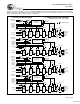
CYV15G0404DXB Evaluation Board Users Guide Figure 4-2 shows the transmitter section of CYV15G0404DXB in more detail. The building blocks of the channel include the phase-align buffer, the 8B/10B encoder and the serializer (shifter). When the reclocker function is enabled, the recovered serial data is reclocked and retransmitted through the serial outputs. Transmit Path Block Diagram REFCLKA+ REFCLKA- RCLK[A..D] are Internal Reclocker Character Clock Signals RED[A..
CYV15G0404DXB Evaluation Board Users Guide Figure 4-3 shows the receive section of the CYV15G0404DXB. The serial data input passes through the clock and data recovery PLL, the deserializer, the framer, the 10B/8B decoder, and the elasticity buffer. When the reclocker function is enabled, the serial data (REDx) and recovered character clock (RCLKx) are passed to the transmitter, where the data is retransmitted. Receive Path Block Diagram RCLK[A..D] are Internal Reclocker Character Clock Signals RED[A..
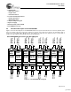
CYV15G0404DXB Evaluation Board Users Guide Figure 4-4 shows the device configuration and control block diagram. The inputs are the external signals WREN, ADDR[3:0], and DATA[7:0] and will be described in subsequent sections. The outputs are the internal signals that are described in Table 5-4. Device Configuration and Control Block Diagram WREN ADDR[3:0] DATA[7:0] Device Configuration and Control Interface = Internal Signal RFMODE[A..D][1:0] RFEN[A..D] FRAMCHAR[A..D] DECMODE[A..D] RXBIST[A..
CYV15G0404DXB Evaluation Board Users Guide 5.0 Board Photograph and Pin Descriptions Figure 5-1 shows the different connectors and pins of the CYV15G0404DXB evaluation board. Table 5-1 provides a description of each connector. Figure 5-1. Photograph of Board with Numbering of Connectors 3.3V (J48) OPTICAL (XT1x) OPT (J25) (DT6) 3.3V LED (see Fig. 5) Channel B I/O (see Fig.
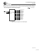
CYV15G0404DXB Evaluation Board Users Guide Figure 5-2 shows the parallel I/O and reference clock connectors for channel A. Channels B, C, and D have a similar layout of connectors. Note that TXERR is not located at the same position for the other channels. Refer to Figure 5-1 for their locations.
CYV15G0404DXB Evaluation Board Users Guide Table 5-1.
CYV15G0404DXB Evaluation Board Users Guide Table 5-1. Description of Connectors of the CYV15G0404DXB Evaluation Board (continued) Connectors Signals Description Power D6 Power Indicator Indicates if the power supply is ON. The LED glows when the power supply is ON. J48 3.3V Banana Jack Connector for power supply to the board DT6 Power Indicator Indicates if the power supply is ON. The LED glows when the power supply is ON. J50 VCC Banana Jack Connector for power supply to the chip • +3.
CYV15G0404DXB Evaluation Board Users Guide Table 5-2.
CYV15G0404DXB Evaluation Board Users Guide Table 5-3. Device Control Latch Description (continued) Pin Name RXCKSELx Characteristics Receive Clock Select • When 1, the associated Output Registers are clocked by REFCLKx • When 0, the associated Output Registers are clocked by the recovered byte clock RXRATEx Receive Clock Rate Select.
CYV15G0404DXB Evaluation Board Users Guide Table 5-3.
CYV15G0404DXB Evaluation Board Users Guide 6.0 Adjusting Settings on the Board To successfully operate the device, the SPDSELx settings and configuration interface must be correctly configured. This section provides directions on how to configure the device. 6.1 Speed Select Jumpers To set the appropriate operating range for each channel’s transmit and receive PLL, jumpers need to be placed on the correct SPDSELx headers for each channel.
CYV15G0404DXB Evaluation Board Users Guide Table 6-1. Device Control Latch Configuration Example ADDR 10 (1010b) 6.
CYV15G0404DXB Evaluation Board Users Guide 7.0 Test Modes The different test modes discussed in this document are BIST, parallel data, and reclocker test modes, including independent clocking on multiple channels. BIST Mode CYV15G0404DXB has the Built-In Self-Test (BIST) capability. Each transmit and receive channel contains an independent BIST Pattern Generator and Checker.
CYV15G0404DXB Evaluation Board Users Guide Cables needed: • SMA to SMA coaxial cables • Power supply cables (banana plug cables). 7.1.1.2 Test Equipment Set-up Figure 7-2 shows the test set-up for BIST on channel A. The signal analyzer in the diagram is optional. See Section 6.4 on page 18 for REFCLKx input options. The BIST tests will use the Crystal Oscillator option.
CYV15G0404DXB Evaluation Board Users Guide Table 7-1.
CYV15G0404DXB Evaluation Board Users Guide Set ULCA = HIGH (Clock & Data Recovery) Set LPENA = LOW Set INSELA = HIGH (Ext. Loopback) (SMA Connectors) Set RCLKENA = LOW (Reclocker Disabled) Figure 7-4. SMA Connectors for External Loopback Mode Figure 7-5. Loop Enable, Use Local Clock, and Input Select DIP Switches Optical Transmission For external loopback with an optical signal, connect an optical module into the optical connector (XT1A). See Figure 7-6.
CYV15G0404DXB Evaluation Board Users Guide 1. Ensure that there are no SMA cables connected to the REFCLKx inputs. Make sure the oscillators are all connected to their respective 14-pin DIP sockets. This test is using the Crystal Oscillator clock option (see Section 6.4 on page 18). Make sure channel A is running at 125 MHz, channel B at 106.25 MHz, channel C at 27 MHz, and channel D at 20 MHz. 2. Adjust Power Supply to 3.3V and 3A limit. Apply power to the board and device. 3.
CYV15G0404DXB Evaluation Board Users Guide Cables needed: • Two SMA-to-SMA coaxial cables • Power supply cables • DG2020 cables with appropriate connectors • Logic analyzer cables with appropriate connectors 7.2.2 Parallel Data Test Set-up For this test, channels A, B, and C will accept parallel data from the DG2020, transmit and receive the data serially in internal loopback mode, and output the same parallel data to the Logic Analyzer.
CYV15G0404DXB Evaluation Board Users Guide the “MORE” button to customize your clock's settings. Your clock definition needs to be changed to the RXCLKA clock to trigger on the faster clock. 7. Adjust the power supply to 3.3V and 3 Amps limit. 8. Apply power to the board and the device. 9. Verify that the power supply LEDs (D6 and DT6) are on. 10.Set SPDSELA = HIGH and SPDSELB = MID. Set ULCx = HIGH, LPENx = HIGH for internal loopback, and RCLKENx = LOW. 11.
CYV15G0404DXB Evaluation Board Users Guide Note. The output of the DG2020 for this PDA file are mapped to POD-A bits 0–11. If outputs need to be remapped for a particular test set-up, consult the DG2020 user’s manual. 2. Using the bit assignment scheme in Table 7-4, connect two TXDATA parallel cables from the DG2020 to J1C and J2C (TXDATA[9:0] to TXDC[7:0] and TXCTC[1:0]). Connect two more TXDATA cables from the DG2020 to J1D and J2D using the same assignment scheme. Table 7-4.
CYV15G0404DXB Evaluation Board Users Guide Table 7-6.
CYV15G0404DXB Evaluation Board Users Guide 7.3.2 Test Equipment Set-up Figure 7-2 shows the test equipment set-up for BIST on channel A and reclocker mode for channel B. 3.3V 3.0A Power Supply 3.3V GND 3.3V Oscilloscope 3.3V GND SEROUTA1 Input RXSTA[2:1] Output Pulse Generator Output Vcc SERINA1 REFCLKA CYV15G0404DXB Evaluation Board REFCLKB SEROUTB1 SERINB1 Figure 7-10. Pictorial Representation of the Reclocker Test Equipment Set-up 7.3.
CYV15G0404DXB Evaluation Board Users Guide Table 7-7.
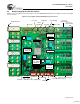
CYV15G0404DXB Evaluation Board Users Guide Appendix A: Schematic Diagram of CYV15G0404DXB Evaluation Board Page 30 of 56 [+] Feedback
CYV15G0404DXB Evaluation Board Users Guide Figure A-1. CYV15G0404DXB Eval Board Top-level Schematic Ch.
CYV15G0404DXB Evaluation Board Users Guide Figure A-2. CYV15G0404DXB Eval Board Top-level Schematic Ch.
CYV15G0404DXB Evaluation Board Users Guide Figure A-3. CYV15G0404DXB Eval Board Top-level Schematic Ch.
CYV15G0404DXB Evaluation Board Users Guide Figure A-4. CYV15G0404DXB Eval Board Top-level Schematic Ch.
CYV15G0404DXB Evaluation Board Users Guide Figure A-5.
CYV15G0404DXB Evaluation Board Users Guide Figure A-6.
CYV15G0404DXB Evaluation Board Users Guide Figure A-7.
CYV15G0404DXB Evaluation Board Users Guide Appendix B: PCB Layout for CYV15G0404DXB Evaluation Board Page 38 of 56 [+] Feedback
CYV15G0404DXB Evaluation Board Users Guide Figure B-1.
CYV15G0404DXB Evaluation Board Users Guide Figure B-2.
CYV15G0404DXB Evaluation Board Users Guide Figure B-3.
CYV15G0404DXB Evaluation Board Users Guide Figure B-4.
CYV15G0404DXB Evaluation Board Users Guide Figure B-5.
CYV15G0404DXB Evaluation Board Users Guide Figure B-6.
CYV15G0404DXB Evaluation Board Users Guide Figure B-7.
CYV15G0404DXB Evaluation Board Users Guide Figure B-8.
CYV15G0404DXB Evaluation Board Users Guide Figure B-9.
CYV15G0404DXB Evaluation Board Users Guide Figure B-10.
CYV15G0404DXB Evaluation Board Users Guide Figure B-11.
CYV15G0404DXB Evaluation Board Users Guide Figure B-12.
CYV15G0404DXB Evaluation Board Users Guide Figure B-13.
CYV15G0404DXB Evaluation Board Users Guide Figure B-14.
CYV15G0404DXB Evaluation Board Users Guide Figure B-15.
CYV15G0404DXB Evaluation Board Users Guide Figure B-16.
CYV15G0404DXB Evaluation Board Users Guide Appendix C: Bill Of Material (BOM) CYV15G0404DXB Evaluation Board Page 55 of 56 [+] Feedback
CYV15G0404DXB Evaluation Board Users Guide Part List, Cypress J1409, Assembly of 10 Boards Item 1 Count 24 2 49 3 9 4 1 5 16 6 9 7 32 8 4 9 6 10 4 RefDes C1A-C1D, C2AC2D, C3A-C3D, C4A-C4D, C5AC5D, C6A-C6D CB10-CB14, CB20-CB51, CB1A-CB1D, CB3A-CB3D, CB5A-CB5D CB2A-CB2D, CB4A-CB4D, CT10 CT20 Compt/ Packg SMDC0603 Description CAP CERAMIC 2200PF 50V X7R 0603 Manufacturer & P/N BC Components: 0603B222K500BT SMDC0805 CAP CERAMIC 0.
Mouser Electronics Authorized Distributor Click to View Pricing, Inventory, Delivery & Lifecycle Information: Cypress Semiconductor: CYV15G0404DX-EVAL