Film-Tech The information contained in this Adobe Acrobat pdf file is provided at your own risk and good judgment. These manuals are designed to facilitate the exchange of information related to cinema projection and film handling, with no warranties nor obligations from the authors, for qualified field service engineers. If you are not a qualified technician, please make no adjustments to anything you may read about in these Adobe manual downloads. www.film-tech.
SDDS Player System DIGITAL FILM SOUND READER DFP-R3000 ® MAINTENANCE MANUAL 1st Edition Serial No.
! WARNING This manual is intended for qualified service personnel only. To reduce the risk of electric shock, fire or injury, do not perform any servicing other than that contained in the operating instructions unless you are qualified to do so. Refer all servicing to qualified service personnel. ! WARNUNG Die Anleitung ist nur für qualifiziertes Fachpersonal bestimmt. Alle Wartungsarbeiten dürfen nur von qualifiziertem Fachpersonal ausgeführt werden.
Table of Contents Manual Structure Purpose of this manual ........................................................................................ 3 (E) Contents ............................................................................................................... 3 (E) Related manuals ................................................................................................... 4 (E) 1. Service Overview 1-1. 1-2. 1-3. 1-4. 1-5. Main Parts Location ...........................................
4. Spare Parts 4-1. 4-2. 4-3. 4-4. Notes on Repair Parts .................................................................................. 4-1 Exploded Views .......................................................................................... 4-2 Electrical Parts List ..................................................................................... 4-8 Accessories Supplied ................................................................................ 4-22 5. Semiconductor Pin Assignments 6.
Manual Structure Purpose of this manual This manual is the Maintenance Manual of the Digital Film Sound Reader DFPR3000. This manual is intended for use by trained system and service engineers, and describes the detailed service information with the intention of servicing based on the component parts (schematic diagrams, board layouts, detailed spare parts list and so on). Contents This manual is organized by following sections. 1.
Related manuals . DFP-R3000/DFP-D3000 Operation Manual (Supplied with the DFPD3000) This manual is necessary for application and operation of the DFP-R3000. . DFP-R3000 Installation Manual (Prepared separately) This manual describes the information when installing DFP-R3000. . DFP-D3000 Maintenance Manual (Prepared separately) This manual describes the inspection of the DFP-D3000 and the information that premise the service based on parts.
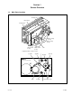
Section 1 Service Overview 1-1. Main Parts Location SE-439 board RD-35 board TG-208 board * LED assembly (P side) LED assembly (S side) SE-437 board (P side) SE-437 board (S side) Lens * Applied Serial No.
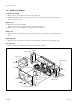
1-2. Removal of Cabinet 1-2. Removal of Cabinet Front panel assembly (1) Remove the two screws (B3 x 4) and four screws (B2.6 x 6). (2) While holding the S2 guide to the direction of the arrow 1, remove the front panel assembly in the direction of the arrow 2. Optics cover (1) Remove the front panel assembly. (Refer to the procedure of the removal of the front panel assembly.) (2) Remove the four screws (PSW3 x 8), and then remove the optics cover.
1-3. Note on RD-35 Board Replacement 1-3. Note on RD-35 Board Replacement 2. Hours meter setting Checking of hours meter The DFP-R3000 serial number and following hours meter setting data are stored in the NVSRAM STK22C48(IC14) on the RD-35 board. The setting data is reset when the RD-35 board or the NVSRAM is replaced. Therefore, set the serial number and the following hours meter again when the RD-35 board or NVSRAM has been replaced.
1-4. LED Function on the Board 1-5. Tools 1-4. LED Function on the Board . RD-35 board D5 (GRN) (B2) : 5 V Light when +5 V power supply is provided correctly D5 (GRN) (H3) : 12 V Light when +12 V power supply is provided correctly . TG-208 board D5 (GRN) (A1) : 12 V Light when +12 V power supply is provided correctly 1-5. Tools Fig. Description Part No. 1 Guide Height Adjustment Tool J-6187-860-A 2 Eccentric Driver (d = ø1.5, D = ø2.
Section 2 Periodic Maintenance and Inspection To make the most of the functions, fully realize the performances of this unit and to lengthen the life of the unit, check and clean the parts every time before film setting, and perform the periodic maintenance. 2-1. Checking and Cleaning before Film Setting We recommend to perform the checking and cleaning for the main components every time before film setting.
2-1.
2-2. Periodic Maintenance Schedule 2-2. Periodic Maintenance Schedule The following table shows the schedule for periodically checking the main parts of the unit to ensure its full functions and performance. It is recommended to use the film running hours of DFP-R3000 as a reference for periodic inspections. The replacing and adjusting of the following parts are described in “Section 3 Mechanical Parts Replacement and Alignment”.
Section 3 Mechanical Parts Replacement and Alignment This section describes the information for the mechanical parts replacement and the required adjustment after the following parts replacement. 1. 2. 3. 4. 5. 6. 7. 8. 9. 10. 11. 12.
Required equipment Equipment Specification Model name Oscilloscope DC to 250 MHz four channels TEKTRONIX 2465B or equivalent DFP-D3000 — — Projector — — Personal computer MS-DOS 5.
3-1. Mechanical Parts Replacement 3-1. Mechanical Parts Replacement 3-1-1. LED assembly (S and P sides) The two LED assemblies use for the S (sound) and P (picture) sides. Required tool L shaped hex. wrench (across ; 2 mm) : 7-770-736-03 1. LED assembly (S-side) 6. Remove the harness from the three hooks of cover support. 7. Disconnect the harnesses of LED assemblies from the connectors (CN5 and CN6) on the RD-35 board, and pull out the harnesses from the hole of base. 8.
3-1. Mechanical Parts Replacement 2. LED assembly (P side) Removal 1. Turn the DFP-R3000 power off. 2. Remove the front panel assembly, drum cover and left side plate. (Refer to the section “1-2. Cabinet Removal”.) 3. Remove the LED assembly (S side). (Perform the procedure 3 through 9 of “Removal of 1. LED assembly (S side)”. 4. Remove he drum assembly. (See the section “3-1-5. Drum assembly”.) 5.
3-1. Mechanical Parts Replacement 3-1-2. Roller guide S1 assembly The height of this roller guide is to be made the reference for the film running. Perform the replacement and the adjustment with care. Required Tools Cleaning cloth : L shaped hex. wrench (across 2 mm) : Screw locking compound : Cleaning fluid : Guide height adjustment tool : Thickness gauge (10 µm) : 10.
3-1. Mechanical Parts Replacement 2. Roller guide S1 height adjustment (3) While holding the bearing retainer, tighten the set screw using the L shaped hex wrench (across 2 mm). Required Tools Cleaning cloth : L shaped hex. wrench (across 2 mm) : Screw locking compound : Cleaning fluid : Guide height adjustment tool : Thickness gauge (10 µm) : 3-184-527-01 7-700-736-03 7-432-114-11 9-919-573-01 J-6187-860-A J-6188-000-A (Required 2 pcs.) Tightening torque : 1.22 ± 0.10 N . m (12 ± 1 kgf .
3-1. Mechanical Parts Replacement 3-1-3. Roller guides S2, S3 and T1 The replacement of the roller guide S2, S3 and T1 are the same. Required Tools Cleaning cloth : 3-184-527-01 Cleaning fluid : 9-919-573-01 Removal 1. Turn the DFP-R3000 power off. 2. Remove the front panel assembly. (Refer to the section “1-2. Cabinet Removal”.) 3. Remove the screw (RK4 x 8) and take out the ornamental washer (ø4), stopper (ø4) and roller guide S2 (or S3 or T1) from the roller guide shaft.
3-1. Mechanical Parts Replacement 3-1-4. Tension regulator holder assembly Required Tools Cleaning cloth : 3-184-527-01 Cleaning fluid : 9-919-573-01 Removal 1. Turn the DFP-R3000 power off. 2. Remove the front panel assembly. (Refer to the section “1-2. Cabinet Removal”.) 3. Remove the tension spring B of the tension regulator B assembly. 4. Remove the three screws (PSW4 x 12) and take out the tension regulator B assembly. 5.
3-1. Mechanical Parts Replacement 3-1-5. Drum assembly Required Tools Cleaning cloth : 3-184-527-01 Cleaning fluid : 9-919-573-01 Removal 1. Turn the DFP-R3000 power off. 2. Remove the front panel assembly, drum cover, and left side plate. (Refer to the section “1-2. Cabinet Removal”.) 3. Remove the LED assembly (S side). Refer to the “1. LED assembly (S side) replacement of section 3-1-1. LED assembly (S and P sides)”. 4. Remove the spring and washer, and pull out the drum assembly from the drum shaft.
3-1. Mechanical Parts Replacement 3-1-6. Sprocket SUB assembly, sprocket holder assembly and brake Required Tools Cleaning cloth : 3-184-527-01 Cleaning fluid : 9-919-573-01 Adjustment/Checking after the replacement After the replacing has been completed, perform the following adjustment and checking. 3-4. Film Running Checking → 3-6. FG Checking → 3-5. Optics Adjustment (S and P side) Removal 1. Turn the DFP-R3000 power off. 2. Remove the front panel assembly. (Refer to the “1-2. Cabinet Removal”.) 3.
3-1. Mechanical Parts Replacement 3-1-7. Film retainer rollers (A and B) Two film retainer rollers A and B are used. Required Tools Cleaning cloth : Molytone grease : Cleaning fluid : Eccentric driver : Thickness gauge : 3-184-527-01 7-662-001-41 9-919-573-01 J-6187-880-A 9-911-053-00 7. Attach the film retainer roller B in the reverse orders of the removal. n Do not apply the coating of the grease to the sprocket and rim of the film retainer rollers A and B.
3-1. Mechanical Parts Replacement 2. Clearance adjustment Required Tools Eccentric driver : J-6187-880-A Thickness gauge : 9-911-053-00 Procedure n Do not damage onto the film running surface of the sprocket by moving the thickness gauge too hard. Sprocket (1) Checking 1 Insert a 0.3 mm thickness gauge between the film retainer rollers (A and B) and the film running surface of the sprocket. While lightly pressing the film retainer rollers in the direction arrow, turn the film retainer rollers.
3-1. Mechanical Parts Replacement (2) Checking 2 Insert a 0.4 mm thickness gauge between the film retainer rollers (A and B) and the film running surface of the sprocket. While lightly pressing the film retainer rollers in the direction arrow, turn the film retainer rollers. In this condition, check that the film retainer rollers do not rotate and that the film retainer rollers and sprocket catch the thickness gauges.
3-1. Mechanical Parts Replacement 3-1-8. CCD (S and P sides) The S and P sides of the CCD are replaced in the same way. n Perform anti-static measures when handling the CCD. Removal 1. Turn the DFP-R3000 power off. 2. Remove the front panel assembly and optics cover. (Refer to the section “1-2. Cabinet Removal”.) 3. Disconnect the harness from the connector (CN1) on the SE-437 board. 4. Remove the two screws (PSW2.6 x 6) fixing the SW437 board. 5.
3-2. Optical Source Adjustment 3-2. Optical Source Adjustment Perform the optical source adjustment when the S and P sides LED assemblies are replaced. n Perform the optical source adjustment with no film loaded. . Adjustment when S side LED assembly is replaced. 1. S side shading adjustment ↓ 3. Shading Compensation (S and P sides) . Adjustment when P (S and P) side LED assembly is replaced. 1. S side shading adjustment ↓ 2. P side shading adjustment ↓ 3.
3-2. Optical Source Adjustment 1. S side shading adjustment Procedure (1) Input the command C1 (press the “C” key and “1” key) from the PC keyboard at the screen of the terminal software started and then press the Enter key. (2) Input the command m0 from the PC keyboard and then press the Enter key. (3) Input the command k0, 70 from the PC keyboard and then press the Enter key.
3-2. Optical Source Adjustment 2. P side shading adjustment Procedure (1) Input the command C1 (press the “C” key and “1” key) from the PC keyboard at the screen of the terminal software started and then press the Enter key. (2) Input the command m100 from the PC keyboard and then press the Enter key. (3) Input the command k1, 70 from the PC keyboard and then press the Enter key.
3-2. Optical Source Adjustment 3. Shading Compensation (S and P sides) Procedure (1) Input the command a from PC and then press the Enter key. (2) Check that the following message (error message in the following table is not displayed) will be displayed on the screen of PC. . Examples of messages n 1. The following are examples of messages displayed when there is no error in the shading compensation. The values of each item differs according to the LED assembly (value after “=”, etc.). 2.
3-3. CCD Bias Adjustment (SE-437 board Adjustment) 3-3. CCD Bias Adjustment (SE-437 board Adjustment) Perform the CCD bias adjustment when CCD and SE-437 board are replaced. Required Equipment and Tools DFP-D3000 Oscilloscope Personal computer: IBM PC/AT compatible Terminal software RS-232C Null modem cable Paper (Thickness ; 0.5 mm or more, size ; 100 x 100 mm) : The paper is able to shut off the light.
3-3. CCD Bias Adjustment (SE-437 board Adjustment) (4) Adjustment Adjust RV1 of the SE-437 (S side) so that a pulse type waveform is generated at A portion of the output waveform. The pulse type waveform appears when RV1 is rotated fully in the clockwise direction and then in the counterclockwise direction. 2. P side adjustment (1) Input the command C1 (press the “C” key and “1” key) from the PC keyboard at the screen of the terminal software started and then press the Enter key.
3-4. Film Running Checking 3-4. Film Running Checking Adjustment Perform the film running checking when roller guides (S1, S2, S3 and T1), sprocket SUB assembly, sprocket holder assembly, brake, tension regulator holder and film retainer roller are replaced. Perform the film running checking with DFP-R3000 installed to the projector. RV1 SE-437 board (P side) (5) After the adjustment has been completed, input the command C0 from the PC keyboard, and then press the Enter key.
3-4. Film Running Checking Procedure (1) Set the sweep times of the oscilloscope so that the pulse width (high level) of the reference pulse (oscilloscope CH2). (2) Check that the deviation A of the output waveform (RF signal) of the oscilloscope CH1 meets the following specifications in respect to the S correction value in the data sheet provided with the alignment film. Specification : A = S correction value ± 0.
3-5. Optics Adjustment 3-5. Optics Adjustment Perform the optics adjustment when roller guides (S1, S2, S3 and T1), tension regulator holder and CCD (SE-437 board) (S and P sides) are replaced. Perform the optics adjustment with DFP-R3000 installed to the projector. Adjustment items (Procedure of S and P sides are the same.
3-5. Optics Adjustment 1. S side optics adjustment (5) Check that the film data width of the oscilloscope CH1 meets the following specification. n By touching against the lens and the protection glass of the CCD adjustment table, do not make them dirty. Specification : Film data width = 6 ± 0.1 scales Step 1. Preparation (1) Load the alignment film into the DFP-R3000 and projector, and then run the alignment film.
3-5. Optics Adjustment Step 3. CCD position adjustment Adjustment (1) Loosen the two screws (PSW2.6 x 6) and four CCD fixing screws (PS2 x 4) on the SE-437 board (S side) abut a half turn. If A portion of the signal leads B portion of the center of the rising pulse more than the correction value, move the CCD from the outside of the optical block to the inside. Adjust by inserting the eccentric screwdriver in the adjustment hole a on the outside of the CCD. Screws (PS 2.
3-5. Optics Adjustment Step 4. CCD azimuth rough adjustment (1) Input the command m10 from the PC keyboard and then press the Enter key. (2) Loosen the S side azimuth fixing screw about a half turn using hex wrench driver (across 2.5 mm). Step 5. CCD focus fine adjustment (1) Connect the filter tool between the TP1 on the RD-35 board and oscilloscope CH1 as shown in the figure.
3-5. Optics Adjustment Step 6. CCD azimuth fine adjustment Step 7. CCD magnification fine adjustment (1) Connect the filter tool between the TP1 on the RD-35 board and oscilloscope CH1 as shown in the figure. (The same as “Step 5. CCD focus fine adjustment”.) (2) Input the command m10 from the PC keyboard and then press the Enter key. (3) Loosen the S side CCD azimuth fixing screw about a half turn using hex wrench driver (across 2.5 mm).
3-5. Optics Adjustment 2. P side optics adjustment (5) Check that the film data width of the oscilloscope CH1 meets the following specification. n By touching against the lens and the protection glass of the CCD adjustment table, do not make them dirty. Specification : Film data width = 6 ± 0.1 scales Step 1. Preparation (1) Load the alignment film into the DFP-R3000 and projector, and then run the alignment film.
3-5. Optics Adjustment Step 3. CCD position adjustment Adjustment (1) Loosen the two screws (PSW2.6 x 6) and four CCD fixing screws (PS2 x 4) on the SE-437 board (P side) about a half turn. If A portion of the signal leads B portion of the center of the rising pulse more than the correction value, move the CCD from the outside of the optical block to the inside. Adjust by inserting the eccentric screwdriver in the adjustment hole a on the outside of the CCD. Screws (PS 2.
3-5. Optics Adjustment Step 4. CCD azimuth rough adjustment (1) Input the command m110 from the PC keyboard and then press the Enter key. (2) Loosen the P side azimuth fixing screw about a half turn using hex wrench driver (across 2.5 mm). Step 5. CCD focus fine adjustment (1) Connect the filter tool between the TP1 on the RD-35 board and oscilloscope CH1 as shown in the figure.
3-5. Optics Adjustment Step 6. CCD azimuth fine adjustment Step 7. CCD magnification fine adjustment (1) Connect the filter tool between the TP1 on the RD-35 board and oscilloscope CH1 as shown in the figure. (The same as “Step 5. CCD focus fine adjustment”.) (2) Input the command m110 from the PC keyboard and then press the Enter key. (3) Loosen the P side CCD azimuth fixing screw about a half turn using hex wrench driver (across 2.5 mm).
3-6. FG checking 3-6. FG checking Perform the FG checking when sprocket SUB assembly, sprocket holder and brake are replaced. (4) Change the measuring range of the oscilloscope as shown below, and check that the FG waveform of the oscilloscope is not chipped.
3-7. Error Rate Checking 3-7. Error Rate Checking Check the error rate using the film for checking error rate. Check the error rate checking with DFP-R3000 installed to the projector and connected to DEP-D3000. (5) Select the “Liner Error Test” command located under the “Test” menu of “DFP-D3000 System Setup” screen.
Section 4 Spare Parts 4-1. Notes on Repair Parts 1. Safety Related Components Warning w Components marked ! are critical to safe operation. Therefore, specified parts should be used in the case of replacement. 2. Standardization of Parts Some repair parts supplied by Sony differ from those used for the unit. These are because of parts commonality and improvement. Parts list has the present standardized repair parts. 3.
CHASSIS, OPTICS BLOCK 4-2. Exploded Views 2 B2.6 x 6 7 TG-208 BOARD 20 12 11 16 PSW 3x6 PSW 3x6 PSW3 x 8 13 B 2.6x6 *1 10 B 3x4 PS2.6 x 6 14 1 SW3 W3 3 PS2 x 4 19 21 PS2 x 5 W3 SW3 BOLT, HEXAGON SOCKET 3 x 10 17 15 8 PS2 x 4 B2.6 x 6 18 5 15 4 6 18 18 14 PSW 3x8 15 PS2 x 8 17 SW3 W3 PSW3 x 8 *1 21 15 17 N3 K2 x 3 TYPE2 K2 x 3 B3 x 4 18 9 17 K 2x3 W3 SW3 W3 SW3 22 W3 SW3 22 B3 x 4 BOLT, HEXAGON SOCKET 3 x 16 B2.
CHASSIS, OPTICS BLOCK No. Part No.
DRUM, LED ASSEMBLY 109 *2 109 *1 *2 112 PSW3 x 15 PSW 3 x 12 PS2.6 x 16 *1 102 104 PSW3 x 15 113 107 107 PS2 x 5 SET SCREW HEXAGON SOCKET 2.
DRUM, LED ASSEMBLY No. 101 102 103 104 105 Part No.
SPROCKET, ROLLER GUIDE, TENSION REGULATOR 219 *1 205 PS2 x 10 W2, SMALL 204 209 226 221 *2 PSW3 x 8 220 225 PSW3 x 8 BOLT.
SPROCKET, ROLLER GUIDE, TENSION REGULATOR No. Part No.
4-3. Electrical Parts List ------------------------------RD-35 BOARD(Board No.Suffix:-12) ------------------------------Ref. No. or Q'ty Part No. SP Description (RD-35 BOARD(Board No.Suffix:-12)) Ref. No. or Q'ty Part No. 1pc A-8318-474-A o MOUNTED CIURCUIT BOARD, RD-35 (This mounted circuit board includes TG-208, DUS-179, DUS-180, DUS-182 boards.
(RD-35 BOARD(Board No.Suffix:-12)) (RD-35 BOARD(Board No.Suffix:-12)) Ref. No. or Q'ty Part No. Ref. No. or Q'ty Part No. SP Description SP Description C152 C160 C161 C162 C163 1-163-038-91 1-163-038-91 1-163-038-91 1-163-038-91 1-163-038-91 25V 25V 25V 25V 25V IC20 IC21 IC22 IC24 IC25 8-759-399-13 8-752-334-64 8-759-528-91 8-759-534-96 8-759-528-92 s s s s s IC IC IC IC IC AD9696KR-REEL CXD1171M DS1000Z-150(TE2) SN74AHCT125PW-E05 TK16111MTL C164 C165 C166 1-163-038-91 s CERAMIC, CHIP 0.
(RD-35 BOARD(Board No.Suffix:-12)) (RD-35 BOARD(Board No.Suffix:-12)) Ref. No. or Q'ty Part No. Ref. No. or Q'ty Part No. SP Description SP Description R22 R23 R24 R25 R27 1-216-657-11 1-216-644-11 1-216-644-11 1-216-660-11 1-216-644-11 s s s s s METAL, METAL, METAL, METAL, METAL, CHIP CHIP CHIP CHIP CHIP 1.8K 0.5% 1/10W 510 0.5% 1/10W 510 0.5% 1/10W 2.4K 0.5% 1/10W 510 0.
------------------------------RD-35 BOARD(Board No.Suffix:-13) ------------------------------Ref. No. or Q'ty Part No. SP Description (RD-35 BOARD(Board No.Suffix:-12)) Ref. No. or Q'ty Part No. SP Description T1 1-475-738-11 s TRANSFORMER, DC-DC CONVERTER TP1 TP2 TP3 TP4 1-535-881-21 1-535-881-21 1-535-881-21 1-535-881-21 X1 1-760-527-11 s OSCILLATOR, CRYSTAL 32.000MHz ------------DUS-179 BOARD ------------Ref. No. or Q'ty Part No.
(RD-35 BOARD(Board No.Suffix:-13)) (RD-35 BOARD(Board No.Suffix:-13)) Ref. No. or Q'ty Part No. Ref. No. or Q'ty Part No. SP Description SP Description C76 C77 C83 C84 C85 1-163-038-91 1-163-038-91 1-163-038-91 1-163-038-91 1-163-038-91 s s s s s CERAMIC, CERAMIC, CERAMIC, CERAMIC, CERAMIC, CHIP CHIP CHIP CHIP CHIP 0.1uF 0.1uF 0.1uF 0.1uF 0.
(RD-35 BOARD(Board No.Suffix:-13)) (RD-35 BOARD(Board No.Suffix:-13)) Ref. No. or Q'ty Part No. Ref. No. or Q'ty Part No.
-----------TG-208 BOARD -----------Ref. No. or Q'ty Part No. (RD-35 BOARD(Board No.Suffix:-13)) Ref. No. or Q'ty Part No. SP Description R187 R188 R189 R190 R191 1-216-061-00 1-216-073-00 1-216-105-91 1-216-105-91 1-216-675-11 s s s s s METAL, METAL, METAL, METAL, METAL, CHIP CHIP CHIP CHIP CHIP 3.3K 5% 1/10W 10K 5% 1/10W 220K 5% 1/10W 220K 5% 1/10W 10K 0.
(TG-208 BOARD) (TG-208 BOARD) Ref. No. or Q'ty Part No. Ref. No. or Q'ty Part No. SP Description SP Description C106 C107 C108 C109 C111 1-135-259-11 1-163-038-91 1-163-038-91 1-163-038-91 1-163-038-91 s s s s s TANTALUM, CHIP 10uF CERAMIC, CHIP 0.1uF CERAMIC, CHIP 0.1uF CERAMIC, CHIP 0.1uF CERAMIC, CHIP 0.1uF 20% 6.
------------------------------RD-35 BOARD(Board No.Suffix:-14) ------------------------------Ref. No. or Q'ty Part No. SP Description (TG-208 BOARD) Ref. No. or Q'ty Part No.
(RD-35 BOARD(Board No.Suffix:-14)) (RD-35 BOARD(Board No.Suffix:-14)) Ref. No. or Q'ty Part No. Ref. No. or Q'ty Part No. SP Description SP Description C115 C116 C117 C118 C119 1-163-038-91 1-135-259-11 1-163-038-91 1-135-259-11 1-163-038-91 s s s s s CERAMIC, CHIP 0.1uF TANTALUM, CHIP 10uF CERAMIC, CHIP 0.1uF TANTALUM, CHIP 10uF CERAMIC, CHIP 0.1uF 25V 25V 25V 25V C120 C121 C122 C123 C124 1-163-038-91 1-135-259-11 1-163-038-91 1-163-038-91 1-163-227-11 s s s s s CERAMIC, CHIP 0.
(RD-35 BOARD(Board No.Suffix:-14)) (RD-35 BOARD(Board No.Suffix:-14)) Ref. No. or Q'ty Part No. Ref. No. or Q'ty Part No.
(RD-35 BOARD(Board No.Suffix:-14)) (RD-35 BOARD(Board No.Suffix:-14)) Ref. No. or Q'ty Part No. Ref. No. or Q'ty Part No. SP Description SP Description R12 R13 R14 R15 R16 1-216-295-91 1-216-644-11 1-216-657-11 1-216-059-00 1-216-644-11 s s s s s METAL, METAL, METAL, METAL, METAL, CHIP CHIP CHIP CHIP CHIP 0 5% 1/10W 510 0.5% 1/10W 1.8K 0.5% 1/10W 2.7K 5% 1/10W 510 0.
(RD-35 BOARD(Board No.Suffix:-14)) (RD-35 BOARD(Board No.Suffix:-14)) Ref. No. or Q'ty Part No. Ref. No. or Q'ty Part No. SP Description SP Description R138 R139 R140 R141 R142 1-216-121-91 1-216-635-11 1-216-672-11 1-216-651-11 1-216-675-11 s s s s s RES, CHIP 1M 5% 1/10W METAL, CHIP 220 0.5% 1/10W METAL, CHIP 7.5K 0.5% 1/10W METAL, CHIP 1K 0.5% 1/10W METAL, CHIP 10K 0.
-----------SE-437 BOARD -----------Ref. No. or Q'ty Part No. (SE-437 BOARD) Ref. No. or Q'ty Part No. SP Description 1pc A-8318-471-A o MOUNTED CIRCUIT BOARD, SE-437 C1 C2 C3 C4 C5 1-163-038-91 1-164-346-11 1-164-346-11 1-164-346-11 1-164-346-11 s s s s s CERAMIC, CHIP 0.
4-4. Accessories Supplied -----------SE-439 BOARD -----------Ref. No. or Q'ty Part No. Ref. No. or Q'ty Part No. SP Description SP Description 1pc 1pc 1pc A-8318-470-A o MOUNTED CIRCUIT BOARD, SE-439 1-695-215-11 o CONTACT, FEMALE 1-764-194-11 o HOUSING, CONNECTOR 4P, FEMALE 1pc 4pcs 1pc 4pcs 1-783-382-11 3-185-981-01 3-194-819-03 7-623-710-57 CN1 1-958-554-13 o HARNESS, SUB (FG1) 5pcs 7-682-963-09 s SCREW +PSW 4X12 PH1 8-759-245-23 s PHOTO REFLECTOR TLP908(LB) ----FRAME ----Ref. No.
Index IC Section 5 Semiconductor Pin Assignments Semiconductors of which functions are equivalent are described here. For parts replacement, refer to the section of Spare Parts in this manual. The circuit diagram of each IC is obtained from the IC data book published by the manufacturer. DIODE Page DA204U ............................ 5-2 DA204UT106 ................... 5-2 RD22FM-T1 ..................... 5-2 RK39 ................................ 5-2 SFPB-74VL ......................
IC Diode, LED, Transistor, Others DIODE TRANSISTOR LED —TOP VIEW— —TOP VIEW— —TOP VIEW— DA204U DA204UT106 CL-150PG-CD ; GREEN CL-150PG-CD-T 2SA1611-M5M6 2SA1611T1-M5M6 1 6 2 5 3 4 1 FC154-TL (SANYO) 6 2 5 4 3 RD22FM-T1 SFPB-74VL TLRH180P —TOP VIEW— 2SC3356-K 2SC3356-T1K 2SC4177-L6 2SC4177-T1L5L6 OTHERS RK39 —TOP VIEW— —TOP VIEW— 2SC2873Y-TE12L 2SD1623-S 1 4 2 3 TLP907-OLB 1 4 2 3 2SJ332S 2SJ332S-TL S 2SK435D (HITACHI) S 5-2 DFP-R3000
IC IC AM29F010-70JC (AMD) 74LCX244SJX (NS)FLAT PACKAGE SN74HCT244ANS (TI)FLAT PACKAGE SN74HCT244ANS-E05 C-MOS 1 M (131,072 x 8)-BIT FLASH EEPROM 2 18 17 16 15 14 13 12 11 2 3 4 5 6 7 8 9 G1 2 18 4 16 6 2 18 4 16 6 14 8 12 11 9 13 7 15 5 17 A Y = A 0 1 x HI-Z G A 0 1 x : : : : Y 0 1 HI-Z LOW LEVEL HIGH LEVEL DON’T CARE HIGH IMPEDANCE 6 28 8 7 27 7 6 8 26 5 9 25 27 26 10 24 23 11 23 25 4 12 22 13 28 29 21 3 2 14 15 16 17 18 19 20 12 22 2
IC CXB1341R (SONY) SERIAL DIGITAL INTERFACE TRANSMISSION ENCODER 17 18 19 20 21 22 23 24 25 26 27 28 29 30 31 32 — — — I — I — I — O O — I I I I NC NC VCCL MDS NC BCAP VCCL ICP GND CPX CPY VCCL FSR0 FSR1 FSR2 FSR3 33 34 35 36 37 38 39 40 41 42 43 44 45 46 47 48 — I I — O I — — O — O — I O I I GND MOD0 MOD1 VCC2 LST THRU GND GND SX VCCS SY VCCL ETS PCK D9X D9Y 49 50 51 52 53 54 55 56 57 58 59 60 61 62 63 64 — I I I I I I I I I I I I I I — VCCT D8X D8Y D7X D7Y D6X D6Y D5X D5Y D4X D4Y D3X D3Y D2X D2Y
IC CY7C199-20VC (CYPRESS)J-LEADED PACKAGE DS1000Z-150(TE2) DS1000Z-25 (DALLAS)FLAT PACKAGE DS1000Z-25(TE2) C-MOS 256 K (32,768 x 8)-BIT SRAM —TOP VIEW— 21 A5 1 VDD 28 23 24 A6 2 27 WE A7 3 26 A4 25 26 1 2 A8 4 25 A3 3 4 A9 5 24 A2 A10 6 23 A1 A11 7 22 OE 5 6 7 8 9 10 A12 8 21 A0 A13 9 20 CE A14 10 19 D7 D0 11 18 D6 D1 12 17 D5 D2 13 16 D4 A0 D0 A1 D1 A2 D2 A3 D3 A4 D4 A5 D5 A6 D6 A7 D7 C-MOS DELAY LINE 12 —TOP VIEW— 13 15 INPUT 1 16 TAP1 VDD 8 TAP2 1
IC KL5C80A12CFP (KAWASAKI STEEL) C-MOS HIGH SPEED 8-BIT MPU 51 VDD VDD 55 60 65 VDD 81 GND GND GND 70 75 GND 80 —TOP VIEW— INPUT 50 GND VDD 85 45 VDD 90 40 GND 95 35 PIN NO. I/O SIGNAL 1 2 3 4 5 6 7 8 9 10 11 12 13 14 15 16 17 18 19 20 21 22 23 24 25 I/O — — I/O I/O I/O O O O O I/O I/O I/O — — — I/O I/O I/O I/O — — I/O O I/O P33/OUTBP2 VDD VDD P32/OUTBP1 P31/SYNC P30/OUTBS0 5-6 EMRD EMWR EIORD EIOWR P27 P26 P25 GND GND GND P24 P23 P22 P21 VDD GND P20 CLK BFSIO 31 VDD GND PIN NO.
IC LM393PS (TI)FLAT PACKAGE LM393PS-E05 MC74HC174AFEL DUAL VOLTAGE COMPARATORS —TOP VIEW— C-MOS D-TYPE FLIP-FLOP WITH RESET —TOP VIEW— 8 VCC 7 3 6 RD IN 5 1 VDD 16 6 Q1 OUT 2 _ + 15 Q6 OUT 11 14 D6 IN 14 13 D1 IN 3 9 + _ 1 4 D2 IN 4 2 3 Q2 D3 Q3 D4 Q4 D5 Q5 D6 Q6 13 D5 IN Q2 OUT 5 EACH FLIP-FLOP 2 INPUTS RD CK D 0 x x 1 0 1 1 1 0 x 5 7 10 12 15 RD D3 IN 6 11 D4 IN 10 Q4 OUT 8 GND Q1 D2 3 2 D —TOP VIEW— CK 1 VCC 16 3 4 GND 15 5 C1_ 3 14 T1 OUT C2+ 4
IC SN74AHCT125PW-E05 STK22C48-S45 IL08 STK22C48-S45 (SIMTEK) C-MOS BUS BUFFER GATES WITH 3-STATE OUTPUT C-MOS (2 K x 8)-BIT NONVOLATILE SRAM —TOP VIEW— —TOP VIEW— 14 VDD 13 12 11 10 9 G 8 10 A Y VCAP 1 VDD 28 9 8 G 0 0 1 1 2 3 4 5 GND 7 6 A 0 1 x Y 0 1 HI-Z 27 WE 2 NC 6 26 HSB A7 3 : : : : 5 4 A6 4 0 1 x HI-Z 7 LOW LEVEL HIGH LEVEL DON’T CARE HIGH IMPEDANCE 25 A8 3 25 A5 5 24 A9 24 21 A4 6 NC 23 1 22 OE A3 7 26 27 A2 8 21 A10 A0 DO0 A1 DO1 A2 DO2 A
IC TK11220BMCL XRD44L60CIV (EXAR) REGULATOR USED FOR POWER SUPPLY C-MOS CCD IMAGE DIGITIZERS —TOP VIEW— V OUT 6 V IN 1 OUT _ + NC 24 23 22 21 20 19 18 17 16 15 14 13 A-GND A-GND A-VDD A-VDD NC 1 2 3 4 5 6 7 8 9 10 11 12 THERMAL PROTECTION _ CONT + V 4 37 38 39 40 41 42 43 44 45 46 47 48 A-VDD V OUT CONT NOISE BYPASS NC NC 4 3 V IN A-GND 1 3 GND 5 2 GND NOISE BYPASS V IN NC 6 1 4 NC NC CONT 36 35 34 33 32 31 30 29 28 27 26 25 —TOP VIEW— 6 BANDGAP REFERENCE 3 NOISE
Section 6 Block Diagram Description The SDDS PLAYER system consists of READER DFPR3000 and DECODER DFP-D3000. The recorded SDDS data in a cinema film is read in READER DFP-R3000 from each S (sound side) track and P (picture side) track by using the CCD. The read SDDS data is processed as a digital signal after waveform equalization, and sent to DECODER DFP-D3000 using a dedicated connection cable. In DECODER DFP-D3000, the sent digitized signal is processed error correction.
Block Diagram OVERALL OVERALL Block Diagram IC24, 26 BUFFER IC25, 27 VCO CXD1171 IC4 EPM7032STC BLKSHS, VCOPWMS CN100 CN100 UNREG 15V IC5, Q1, Q2 DC-DC CONVERTER CN4 12V IC1 78L12 VIDEO IC2 CCD Q2-12 CCD DRIVER S side block Offset & Gain CCDS 8 Analog DATA Reproduce PLL EQ Clamp SPHRS, SSHP, SCLAMP IC7 PH1, PH2, PHT, PHRS IC2 TK11220 IC38, CXD9067Q (SDDS GA) CCDS IC6 XRD4460 AD CN100 CN100 64 M UNREG 15V UNREG 15V TG-208 (3/4) 16 M IC9 CLK CN1 LED (S-side) IC22 DL IMGOUTS
Block Diagram OVERALL OVERALL Block Diagram IC24, 26 BUFFER DFP-R3000 : S/N 10601 and higher 64 M IC32 CLK IC20 CP FL1 LPF CXD1171 IC22 DL SDCLK IC21 DA CPINS RD-35 (Suffix : -14) DCPINS VCOUPS, VCODNS, VCOOUTS IC25, 27 VCO IC45 EPM7032STC 16 M IMGOUTS IC2 TK11220 BLKSHS, VCOPWMS S-side IC38, CXD9067Q (SDDS GA) CN4 CN1 LED (S-side) 12V IC1 78L12 S side block Offset & Gain UNREG 17V UNREG 17V CCDS VIDEO IC2 CCD Q2-12 CCD DRIVER Shading Adjust IC7 PH1, PH2, PHT, PHRS IC3
SE-437 Section 7 Board Layouts Index Board name Circuit function Page RD-35 7-2 SE-437 7-2 SE-439 7-6 TG-208 7-8 SE-437 SE-437 -B SIDESUFFIX : -12 -A SIDESUFFIX : -12 DFP-R3000 (SY) : S/N 10001 to 10150 E1 7-1 7-1 C8 C9 R23 R3 R4 R32 Q3 R29 C13 C12 R10 Q6 Q2 R24 C28 R27 C29 R14 C18 R22 C27 R28 R25 Q7 R19 C22 R21 R8 R7 R16 R20 IC1 C21 C1 R30 C30 C25 C31 C19 Q12 Q11 SE-437 -A SIDE- SE-437 -B SIDE- SUFFIX : -13 SUFFIX : -13 DFP-R3000 (SY) : S/N 10151 and Higher DFP-R300
DUS-179, DUS-180, DUS-182, RD-35 RD-35, DUS-182, DUS-180, DUS-179 —————————————————— RD-35 (SUFFIX:-12) —————————————————— RD-35 -A SIDE- DFP-R3000 (SY) : S/N 10001 to 10150 SUFFIX : -12 DUS-179 -B SIDE- DUS-180 -B SIDE- DUS-182 -B SIDE- SUFFIX : -11 SUFFIX : -11 SUFFIX : -11 DFP-R3000 (SY) : S/N 10001 to 10150 DFP-R3000 (SY) : S/N 10001 to 10150 DFP-R3000 (SY) : S/N 10001 to 10150 7-2 7-2 CN4 CN5 CN6 CN7 CN8 CN9 H4 H3 H2 B1 H4 A2 D1 D2 D3 D4 D5 D6 D7 D8 D9 D10 D11 D12 D13 D14 C4 * B4 *
RD-35 RD-35 RD-35 -B SIDESUFFIX : -12 DFP-R3000 7-3 7-3
RD-35 RD-35 —————————————————— RD-35 (SUFFIX:-13) —————————————————— RD-35 -A SIDE- DFP-R3000 (SY) : S/N 10151 to 10600 SUFFIX : -13 7-4 7-4 CN2 CN4 CN5 CN6 CN7 CN8 CN9 H1 H4 H3 H2 B1 H4 A2 D1 D2 D3 D4 D5 D6 D7 D8 D9 D10 D11 D12 D13 D14 C4 * B4 * B5 C5 B2 H3 * G3 * G2 G2 G2 * F1 * E5 H3 H2 E1 E2 E3 E4 E5 E6 E7 E8 E9 E10 E11 E12 E13 E14 H4 G4 H5 F4 A2 A3 C3 A1 A5 E1 E5 F2 G1 C1 IC1 IC2 IC3 IC4 IC5 IC6 IC7 IC8 IC9 IC10 IC11 IC12 IC13 IC14 IC15 IC16 IC17 IC18 IC19 IC20 IC21 IC22 IC23 IC24 IC25 IC
RD-35 RD-35 RD-35 -B SIDESUFFIX : -13 DFP-R3000 7-5 7-5
SE-439, RD-35 C143 L6 IC18 R129 E14 C90 IC41 C3 IC1 IC27 IC42 Q9 C60 IC10 D14 Q8 IC43 IC32 CN5 C59 IC40 R231 C70 R9 C153 R10 C154 R230 IC6 C138 C134 R81 R83 R88 R87 Z39 R76 R232 C172 Z36 R97 C176 Z37 R235 C171 Z38 C127 Z34 G1 H1 H3 H3 H2 B1 H5 A2 D1 D2 D3 D4 D5 D6 D7 D8 D9 D10 D11 D12 D13 D14 C4 * B4 * B5 C5 B2 H3 * G3 * G2 G2 G2 * F1 * E5 H3 H2 E1 E2 E3 E4 E5 E6 E7 E8 E9 E10 E11 E12 E13 E14 H4 H5 G3 G5 A2 A3 C3 A1 A5 E1 E4 F2 G1 C1 FB1 FB2 B4 B3 C67 IC44 C144 IC33 C73 F
DFP-R3000 R86 C66 R82 C62 C65 C179 R242 C130 C121 R156 C189 R163 C187 7-7 C7 R160 C4 C123 C28 C126 C10 R37 R35 R30 R27 R23 R19 R16 R11 C163 R4 R64 C38 C165 R59 R49 R43 C119 R158 R159 C122 7-7 C12 C74 C177 C86 R121 R118 R120 R188 C112 R66 R65 C22 R114 R119 R113 R112 C76 R244 C100 R148 R142 R144 R149 C184 C102 C101 C83 C85 R106 R109 R110 C77 R127 R128 R238 R239 R240 C88 R60 R62 Q4 R245 C181 D11 R138 Q14 C116 R53 Q6 C14 Q1 C40 C33 C31 C30 C84 Q3 C16 C
TG-208 TG-208 D5 R31 IC34 L8 IC26 IC35 C1 IC24 IC30 IC36 C3 C69 C4 Z9 Z4 Z5 Z7 E6 TP6 Z26 Z27Z28 Z29Z30 E7 TP1 IC4 IC22 IC20 IC12 L1 IC31 IC29 C7 TG-208 -A SIDE- DFP-R3000 (SY) : S/N 10001 to 10600 SUFFIX : -11 R18 R1 Q2 C82 CN100 R20 R82 R89 R90 C28 C10 C16 C11 C158 C72 C62 IC9 C155 C169 C63 R17 C18 C19 R4 R5 R77 R78 R97 R16 C156 C176 R76 C172 C21 C67 C66 R86 C27 C29 R11 R13 C64 SUFFIX : -11 7-8 D1 D2 D3 D4 D5 D7 D8 D11 D12 * D1 * D1 * D1 * D1 A1 * D2 * D2 * B2 *
Section 8 Schematic Diagrams 1 Index Board name Circuit function Page RD-35 8-2 SE-437 8-14 TG-208 8-11 Frame 8-15 2 3 4 5 8-1 DFP-R3000 A B C D 8-1 E F G H
RD-35 (1/4) RD-35 (1/4) DFP-R3000 (SY) : S/N 10001 to 10150 (Board No. Suffix -12) DFP-R3000 (SY) : S/N 10151 to 10600 (Board No. Suffix -13) R20 1 C37 22 16V C34 C35 C36 0.1 0.1 0.1 CCDS9 CCDS8 3.3V ADEN_CAL 1 ADSCLK ADRESET ADXSTYB *3 -2 12V IC41 NJM78L12UA-TE1 3 IN R26 10 1/10W C147 10 50V OUT 1 GND C148 0.1 C150 10 50V C149 0.1 2 Z10 -2 -2 -2 ADSDI C48 0.1 R54 10k R48 100 C55 0.1 C50 0.01 C157 10p -2 C45 0.
RD-35 (2/4) RD-35 (2/4) DFP-R3000 (SY) : S/N 10001 to 10150 (Board No. Suffix -12) DFP-R3000 (SY) : S/N 10151 to 10600 (Board No. Suffix -13) 1 5V-4 72 71 70 69 68 67 66 65 64 63 62 61 60 59 58 57 56 55 54 53 52 51 50 49 48 47 46 45 44 43 42 41 40 39 38 37 D0 D1 D2 D3 D4 D5 D6 D7 C163 0.1 FG TRIG CENTER DAOUT0 DAOUT1 DAOUT2 DAOUT3 C164 0.
RD-35 (3/4) RD-35 (3/4) DFP-R3000 (SY) : S/N 10001 to 10150 (Board No. Suffix -12) DFP-R3000 (SY) : S/N 10151 to 10600 (Board No. Suffix -13) 1 1 2,4 BUS C83 0.1 C84 0.1 5V C85 0.1 5V C86 0.1 C88 0.1 C87 0.1 5V C89 0.1 5V C90 0.
RD-35 (4/4) RD-35 (4/4) DFP-R3000 (SY) : S/N 10001 to 10150 (Board No. Suffix -12) DFP-R3000 (SY) : S/N 10151 to 10600 (Board No. Suffix -13) 5V IC2 TK11220BMCL C12 C13 C14 C15 C16 C17 C18 C19 0.1 0.1 0.1 0.1 0.1 0.1 0.1 0.1 1 VIN 6 CNT C9 0.1 N.B GND 2 3 1 C10 0.1 C22 0.1 C11 100 25V 5V FB1 C8 100 25V C20 C21 0.1 0.
RD-35 (1/5) RD-35 (1/5) C37 22 16V C34 C35 C36 0.1 0.1 0.1 SE-437(S SIDE),CN1 R20 1 CCDS9 CCDS8 R41 0 -2 R26 10 1/10W C38 22 C39 16V 0.1 SCCDPWR -2 -2 -2 R48 100 C50 0.01 C157 10p -2 12 11 10 9 8 7 6 5 4 3 2 1 NC NC DB7 DB6 DB5 DVDD DGND DB4 DB3 DB2 N.C. N.C. IC6 XRD44L60CIV NC DB1 DB0 UNDER SYNC VDD CK_POL GND RSTCCD SHP SHD CLAMP C45 0.
RD-35 (2/5) RD-35 (2/5) DFP-R3000 (SY) : S/N 10601 and Higher R130 10k 5V 5V-2 FL1 1 2 3 4 5 6 7 8 9 L7 10µH IMGOUTS0 IMGOUTS1 IMGOUTS2 IMGOUTS3 IMGOUTS4 IMGOUTS5 IMGOUTS6 IMGOUTS7 XCLK D0 D1 D2 D3 D4 D5 D6 D7 BLK DVSS VB CLK DVDD DVDD AVDD -IO IO AVDD AVDD VG VRFG IREF AVSS DVSS 10 50V 18 24 23 22 21 20 19 18 17 16 15 14 13 16 15 13 12 C105 0.1 C104 0.1 IC20 AD8561AR-REEL7 5V C107 0.1 C106 10 10 R131 1k 3 15 2 8 7 8 R133 1k 4 Q14 2SK1070PIDTL S C109 R136 0.
RD-35 (3/5) RD-35 (3/5) DFP-R3000 (SY) : S/N 10601 and Higher 1 CPINS DCPINS CCDS0 IMGOUTS5 IMGOUTS6 IMGOUTS7 PLED SLED PVSYNC SVSYNC VCOOUTS VCOPWMS SDCLK SLEDCUR PLEDCUR IOWR 3.3V-2 BLKSHS IMGOUTS0 IMGOUTS1 IMGOUTS2 IMGOUTS3 IMGOUTS4 C161 0.1 BUS A2 A1 A0 IORD 4,5 ADEN_CAL C162 0.1 1,2 72 71 70 69 68 67 66 65 64 63 62 61 60 59 58 57 56 55 54 53 52 51 50 49 48 47 46 45 44 43 42 41 40 39 38 37 D0 D1 D2 D3 D4 D5 D6 D7 C163 0.
RD-35 (4/5) RD-35 (4/5) DFP-R3000 (SY) : S/N 10601 and Higher 1 1,2 3,5 BUS C83 0.1 C84 0.1 5V C85 0.1 5V 5V 5V C89 0.1 C86 0.1 C88 0.1 C87 0.1 C90 0.1 IC11 CY7C199-20VC 32 84 61 53 52 44 34 21 3 2 Z17 Z18 Z19 Z20 Z21 Z22 Z23 Z24 Z4 Z5 Z6 Z7 R118R119R120R121R122R123R124 5V 10k 10k 10k 10k 10k 10k 10k Z8 Z9 1/10W 1/10W 1/10W 1/10W 1/10W 1/10W 1/10W P31 P30 R117 10k 1/10W R220 0 R221 0 R222 0 R223 0 R224 0 R225 0 R226 0 ,NM R227 0 ,NM R175 3.3k R150 3.
RD-35 (5/5) RD-35 (5/5) DFP-R3000 (SY) : S/N 10601 and Higher 5V IC2 TK11220BMCL 1 1 VIN 6 CNT C8 100 25V VOUT 4 N.B GND 3 2 C9 0.1 C10 0.1 C22 0.1 C12 C13 C14 C15 C16 C17 C18 C19 0.1 0.1 0.1 0.1 0.1 0.1 0.1 0.1 C11 100 25V C20 C21 0.1 0.
TG-208 (1/3) DFP-R3000 (SY) : S/N 10001 to 10600 TG-208 (1/3) C37 22 16V C34 C35 C36 0.1 0.1 0.1 SE-437(S SIDE),CN1 CCDS9 CCDS8 ADEN_CAL R20 1 1 -2 (UNREG17V) 12V R26 10 1/10W Z20 CN4 9 SCCDPWR -2 -2 -2 C55 0.1 C52 0.01 B -2 R54 10k SVIDEO(X) SVIDEO(GND) R48 100 C50 0.01 C157 10p C38 22 16V 24 23 22 21 20 19 18 17 16 15 14 13 -2 C45 0.1 NC LOAD SDI VRT VRTO VDD IN_NEG IN_POS GND VRBO VRB NC NC NC DB7 DB6 DB5 DVDD DGND DB4 DB3 DB2 N.C. N.C.
TG-208 (2/3) TG-208 (2/3) DFP-R3000 (SY) : S/N 10001 to 10600 TP1 5V R130 10k 5V-2 L7 10µH 1 1 2 3 4 5 6 7 8 9 10 11 12 IMGOUTS0 IMGOUTS1 IMGOUTS2 IMGOUTS3 IMGOUTS4 IMGOUTS5 IMGOUTS6 IMGOUTS7 XCLK D0 D1 D2 D3 D4 D5 D6 D7 BLK DVSS VB CLK DVDD DVDD AVDD -IO IO AVDD AVDD VG VRFG IREF AVSS DVSS C133 10 16V 24 23 22 21 20 19 18 17 16 15 14 13 5V-2 IC20 AD9696KR-REEL IC21 CXD1171M-TH FL1 5V C107 C105 0.1 12 10 9 TP2 C106 10 14 13 R131 1k 3 15 2 0.
TG-208 (3/3) TG-208 (3/3) DFP-R3000 (SY) : S/N 10001 to 10600 1 1,2 BUS 5V 5V 3.
SE-437 SE-437 DFP-R3000 (SY) : S/N 10001 and Higher 1 *Board No.Suffix-12 12V R23 6.8k ,NM Q2 FC154-TL 1 R9 2.7 2 3 6 C2 1 6 C14 10 16V 5 C6 270p CN1 6 5 R1 22 R10 22 4 4 1 XPH1 1 C7 180p R2 22 2 2 3 6 2 5 3 Q1 FC154-TL Q4 FC154-TL 4 12V 1 Q5 FC154-TL R12 2.7 2 3 6 RV1 5k C3 1 6 C15 10 16V * 5 C8 270p CN1 7 5 R3 22 4 4 1 XPH2 1 VDD 1 C9 180p R4 22 12V IC2 RL0256DEG-011 R13 22 2 R21 3.9k 2 C23 C24 10 C25 C26 10 16V 1 1 16V R23 R24 R14 R25 1k 5.6k 1.5k 7.
FRAME FRAME DFP-R3000 (SY) : S/N 10001 to 10600 1 S-side LED (S-side) CN100 CN100 ! HN101 TLRH180P VIDEO(GND) VIDEO(X) VCC GND XPHT XPH1 XPH2 XPHRS CCDPWR CN1 1 2 4 3 5 6 7 8 9 CN4 1 2 4 3 5 6 7 8 9 SVIDEO(GND) SVIDEO(X) VCC(UNREG17V) GND XSPHT XSPH1 XSPH2 XSPHRS SCCDPWR 24V NC GND GND SDI(X) SDI(G) W1 1 2 3 4 A1 G1 3 2 A1 G1 4 1 2 – EXT VIEW – TG-208 (1/2) SE-437 HN104 CN6 1 SLED(A) 2 SLED(K) 3 SLED(G) P-side LED (P-side) 3 CN100 CN100 ! HN102 TLRH180P VIDEO(GND) VIDEO(X) VCC GND X
FRAME FRAME DFP-R3000 (SY) : S/N 10601 and Higher 1 S-side LED (S-side) ! HN101 TLRH180P VIDEO(GND) VIDEO(X) VCC GND XPHT XPH1 XPH2 XPHRS CCDPWR 2 CN1 1 2 4 3 5 6 7 8 9 CN4 1 2 4 3 5 6 7 8 9 SVIDEO(GND) SVIDEO(X) VCC(UNREG17V) GND XSPHT XSPH1 XSPH2 XSPHRS SCCDPWR W1 1 2 3 4 A1 G1 24V NC GND GND SDI(X) SDI(G) 3 2 A1 G1 4 1 – EXT VIEW – SE-437 HN104 CN6 1 SLED(A) 2 SLED(K) 3 SLED(G) P-side LED (P-side) 3 ! HN102 TLRH180P VIDEO(GND) VIDEO(X) VCC GND XPHT XPH1 XPH2 XPHRS CCDPWR CN1 1 2 4 3
The material contained in this manual consists of information that is the property of Sony Corporation and is intended solely for use by the purchasers of the equipment described in this manual. Sony Corporation expressly prohibits the duplication of any portion of this manual or the use thereof for any purpose other than the operation or maintenance of the equipment described in this manual without the express written permission of Sony Corporation.
DFP-R3000 (SY) J, E 9-968-523-01 Sony Corporation Broadcasting & Professional Systems Company Printed in Japan 1998.