
Static RAM Specification Sheet
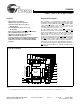
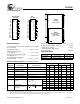

CY62256
Document #: 38-05248 Rev. *B Page 3 of 11
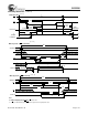
I
SB2
Automatic CE
Power-down Current—
CMOS Inputs
Max. V
CC
, CE > V
CC
− 0.3V
V
IN
> V
CC
− 0.3V, or V
IN
<
0.3V, f = 0
15 1 5 mA
L2502 50 µA
LL 0.1 5 0.1 5 µA
Indust’l Temp Range LL 0.1 10 0.1 10 µA
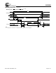
Capacitance
[4]
Parameter Description Test Conditions Max. Unit
C
IN
Input Capacitance T
A
= 25°C, f = 1 MHz,
V
CC
= 5.0V
6 pF
C
OUT
Output Capacitance 8 pF
Electrical Characteristics Over the Operating Range (continued)
Parameter Description Test Conditions
CY62256−55 CY62256−70
UnitMin. Typ.
[3]
Max. Min. Typ.
[3]
Max.
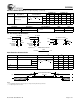
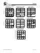
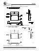
AC Test Loads and Waveforms
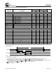
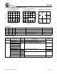
Data Retention Characteristics
Parameter Description Conditions
[5]
Min. Typ.
[3]
Max. Unit
V
DR
V
CC
for Data Retention 2.0 V
I
CCDR
Data Retention Current L V
CC
= 3.0V, CE > V
CC
− 0.3V,
V
IN
> V
CC
− 0.3V, or V
IN
< 0.3V
2 50 µA
LL 0.1 5 µA
LL Ind’l 0.1 10 µA
t
CDR
[4]
Chip Deselect to Data Retention Time 0 ns
t
R
[4]
Operation Recovery Time t
RC
ns
Data Retention Waveform
Notes:
4. Tested initially and after any design or process changes that may affect these parameters.
5. No input may exceed V
CC
+ 0.5V.
3.0V
5V
OUTPUT
R1 1800
Ω
R2
990Ω
100 pF
INCLUDING
JIG AND
SCOPE
GND
90%
10%
90%
10%
<5ns
<5ns
5V
OUTPUT
R1 1800
Ω
R2
990Ω
5pF
INCLUDING
JIG AND
SCOPE
(a) (b)
OUTPUT 1.77V
Equivalent to: THÉ VENIN EQUIVALENT
ALL INPUT PULSES
639Ω
3.0V3.0V
t
CDR
V
DR
> 2V
DATA RETENTION MODE
t
R
CE
V
CC