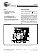
CY62256
Document #: 38-05248 Rev. *B Page 6 of 11
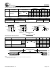
Note:
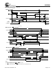
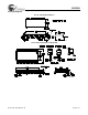
16. During this period, the I/Os are in output state and input signals should not be applied.
Switching Waveforms (continued)
DATA I/O
ADDRESS
t
HD
t
SD
t
LZWE
t
SA
t
HA
t
AW
t
WC
CE
WE
t
HZWE
DATA
IN
VALID
Write Cycle No. 3 (WE Controlled, OE LOW)
[10, 15]
NOTE 16