
Static RAM Specification Sheet


8K x 8 Static RAM
CY7C185
Cypress Semiconductor Corporation • 3901 North First Street • San Jose • CA 95134 • 408-943-2600
Document #: 38-05043 Rev. *A Revised September 13, 2002
185
Features
• High speed
—15 ns
•Fast t
DOE
• Low active power
— 715 mW
• Low standby power
— 220 mW
• CMOS for optimum speed/power
• Easy memory expansion with CE
1
, CE
2
, and OE features
• TTL-compatible inputs and outputs
• Automatic power-down when deselected
Functional Description
[1]
The CY7C185 is a high-performance CMOS static RAM orga-
nized as 8192 words by 8 bits. Easy memory expansion is
provided by an active LOW chip enable (CE
1
), an active HIGH
chip enable (CE
2
), and active LOW output enable (OE) and
three-state drivers. This device has an automatic power-down
feature (CE
1
or CE
2
), reducing the power consumption by 70%
when deselected. The CY7C185 is in a standard 300-mil-wide
DIP, SOJ, or SOIC package.
An active LOW write enable signal (WE
) controls the writ-
ing/reading operation of the memory. When CE
1
and WE in-
puts are both LOW and CE
2
is HIGH, data on the eight data
input/output pins (I/O
0
through I/O
7
) is written into the memory
location addressed by the address present on the address
pins (A
0
through A
12
). Reading the device is accomplished by
selecting the device and enabling the outputs, CE
1
and OE
active LOW, CE
2
active HIGH, while WE remains inactive or
HIGH. Under these conditions, the contents of the location ad-
dressed by the information on address pins are present on the
eight data input/output pins.
The input/output pins remain in a high-impedance state unless
the chip is selected, outputs are enabled, and write enable
(WE
) is HIGH. A die coat is used to insure alpha immunity.
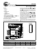
Logic Block Diagram Pin Configurations
A
1
A
2
A
3
A
4
A
5
A
6
A
7
A
8
A
0
A
10
A
9
A
11
A
12
I/O
0
1
2
3
4
5
6
7
8
9
10
11
12
13
14
28
27
26
25
24
23
22
21
20
19
18
17
16
15
V
CC
WE
CE
2
A
3
A
2
A
1
OE
A
0
CE
1
I/O
7
I/O
6
I/O
5
I/O
4
I/O
3
NC
A
4
A
5
A
6
A
7
A
8
A
9
A
10
A
11
A
12
I/O
0
I/O
1
I/O
2
GND
256 x 32 x 8
ARRAY
INPUT BUFFER
COLUMN DECODER
ROW DECODER
SENSE AMPS
POWER
DOWN
I/O
1
I/O
2
I/O
3
I/O
4
I/O
5
I/O
6
I/O
7
CE
1
CE
2
WE
OE
Top View
DIP/SOJ/SOIC
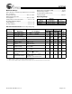
Selection Guide
[2]
7C185-15 7C185-20 7C185-25 7C185-35
Maximum Access Time (ns) 15 20 25 35
Maximum Operating Current (mA) 130 110 100 100
Maximum Standby Current (mA) 40/15 20/15 20/15 20/15
Note:
1. For guidelines on SRAM system design, please refer to the ‘System Design Guidelines’ Cypress application note, available on the internet at www.cypress.com.
2. For military specifications, see the CY7C185A data sheet.