Getting Started with CapSense® Document No. 001-64846 Rev. *A Cypress Semiconductor 198 Champion Court San Jose, CA 95134-1709 Phone (USA): 880.858.1810 Phone (Intnl): 408.943.2600 http://www.cypress.
Copyrights Copyrights © Cypress Semiconductor Corporation, 2010-2011. The information contained herein is subject to change without notice. Cypress Semiconductor Corporation assumes no responsibility for the use of any circuitry other than circuitry embodied in a Cypress product. Nor does it convey or imply any license under patent or other rights.
Contents 1. Introduction.................................................................................................................................................................... 6 1.1 How to Use This Guide .......................................................................................................................................... 6 1.2 Cypress CapSense Products ......................................................................................................................
3. Design Considerations ............................................................................................................................................... 29 3.1 3.2 3.3 3.4 3.5 3.6 3.7 4. CapSense Product Portfolio ....................................................................................................................................... 55 4.1 5. Selecting the Right CapSense Device ..........................................................................................
6.2 6.3 6.4 7. CY8C21x34/B / CY8C24x94 to CY8C20xx6A/H.................................................................................................. 60 CY8C20xx6A/H to CY8C21x34/B / CY8C24x94.................................................................................................. 60 Pin-to-Pin Compatibility ....................................................................................................................................... 61 Resources .......................................
1. Introduction 1.1 How to Use This Guide This document is the starting point for any new CapSense design. The most important thing the guide does is to help you to select the right device for your application using our CapSense Selector Guide in Chapter 5.
1.3 Document Revision History Revision Issue Date Origin of Change Description of Change ** 12/17/2010 SSHH New Guide *A 3/4/2011 SSHH Multiple chapter enhancements for content and reader clarity 1.4 Document Conventions Convention Usage Courier New Displays file locations, user entered text, and source code: C:\ ...cd\icc\ Italics Displays file names and reference documentation: Read about the sourcefile.hex file in the PSoC Designer User Guide.
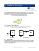
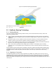
2. CapSense Technology Cypress’s CapSense controllers use changes in capacitance to detect the presence of a finger on or near a touch surface, as shown in Figure 2-1. This capacitive sensor example illustrates a touch sensor replacement for a mechanical button. This sensing function is achieved using a combination of hardware and firmware. The following section provides an overview of capacitive sensing technology and CapSense solutions. Figure 2-1. Illustration of a Capacitance Sensor Application 2.
2.1.2 Mutual Capacitance Mutual capacitance uses a pair of pins and measures the capacitance between those pins. A mutual-capacitance system operates by driving a current on a transmit pin and measuring the charge on a receive pin. When a finger is placed between the transmit and receive pins it decreases the measured capacitance. The mutual-capacitance effect is best suited to multitouch systems, such as touch screens and track pads.
Figure 2-4. CapSense System Equivalent Model With a finger on the sensor surface, C X equals the sum of C P and C F . 𝐶𝑋 = 𝐶𝑃 + 𝐶𝐹 Equation 2 2.3 CapSense Sensing Technology 2.3.1 Sensing Methods There are a number of capacitive sensing methods currently in use across the electronics industry. Some of the major sensing methods include: Charge Transfer: Incremental packets of charge are transferred between the sensor capacitor and a reference capacitor until a reference voltage is reached.
Figure 2-5. Output of Sensing Algorithm 2.3.3 CapSense with Sigma Delta Modulator (CSD) Cypress’s CSD method uses a switched capacitor circuit on the front end of the system to convert the sensor capacitance to an equivalent resistor, as shown in Equation 3. A Sigma-Delta modulator converts the current measured through the equivalent resistor into a digital count. When a finger is on the sensor, the capacitance increases and the equivalent resistance decreases.
Figure 2-7. CSD Equivalent Circuit 𝑅𝑒𝑞 = 1 Equation 3 𝑓𝑠𝑤 ×𝐶𝑃 Where: f SW = switching frequency C P = sensor capacitance For an in-depth discussion of Cypress’s CSD sensing method refer to PSoC® CY8C20x66, CY8C20x66A, CY8C20x46/96, CY8C20x46A/96A, CY8C20x36, CY8C20x36A Technical Reference Manual (TRM). 2.3.
Figure 2-9. CSA_EMC Equivalent Circuit The CSA_EMC CapSense algorithm has been enhanced to work well in the presence of RF interference. CSA_EMC is used in applications where CapSense is exposed to conducted interference, AC noise, and other noise sources such as inverters, transformers, and power supplies. Electromagnetic Compatibility (EMC) Considerations discusses this topic in detail.
2.4.1 Signal-to-Noise Ratio (SNR) Figure 2-10. Signal and Noise One of the main goals of tuning a CapSense system is to reliably discriminate between TOUCH and NO TOUCH sensor states. The signal is the change in the sensor response when a finger is placed on the sensor. The change in the sensor response refers to a trend in the raw counts called the Baseline. This reference level is continuously updated when a finger is not on the sensor.
2.5 Sensor Types Capacitive sensors can be broadly classified into four categories: buttons, sliders, touchscreens, and proximity sensors. Different sensor types cater to different market segments Figure 2-11. Types of Capacitive Sensors Button (Zero-dimensional) Slider (One-dimensional) Touchscreen and Trackpad (Two-dimensional) Proximity (Three-dimensional) 2.5.
2.5.1.2 Matrix Buttons In applications requiring a high number of buttons such as a calculator keypad or a QWERTY keyboard, capacitive sensors can be arranged in a matrix. This allows a design to have more buttons than there are I/O pins on the CapSense controller. Figure 2-13. Typical Matrix Buttons A matrix button design consists of two groups of capacitive sensors: Row sensors and Column sensors.
2.5.2.1 Linear Sliders In a linear slider each CapSense controller I/O pin is connected to one slider segment. A zigzag pattern (double chevron) is recommended for slider segments. This layout ensures that when a segment is touched, the adjacent segments are also partially touched. Sensor data from multiple sensors improves the estimate of the finger position. The maximum number of slider segments is a function of the number of available CapSense controller pins and the required response time. Figure 2-14.
2.5.2.3 Radial Sliders Radial sliders are similar to linear slider in that finger position is estimated using data from adjacent sensors, however, radial sliders are continuous (no beginning or end). Figure 2-16. Radial Slider Area contacted by finger 2.5.3 Touchscreens and Trackpads (Two-Dimensional Sensors) Cypress’s TrueTouch™ touchscreen solutions use mutual capacitance sensing. Visit TrueTouch™ Touch Screen Controllers to learn about these products. Cypress also offers trackpad solutions.
2.6 Sensor Construction 2.6.1 Field Coupled via Copper Trace (PCB) Figure 2-18. Field Coupled Using PCB Features of a PCB-based design: Most common implementation Copper pads etched on the surface of the PCB act as sensor pads Electric field emanates from the copper sensor pad to ground plane No mechanical moving parts A nonconductive overlay serves as the touch surface for the button Ideal topology for simple flat panel designs Low BOM cost 2.6.
Features of a design based on springs/gaskets/foam: Electrical field coupled from PCB to overlay using a compressed spring, or conductive gasket or foam Conductive material itself acts as capacitive sensor pad No mechanical moving parts.
Figure 2-20. LED Sourcing and Sinking Configuration VDD R Vsrc CapSense Controller Vsnk LED CapSense button R CapSense Controller CapSense button Vsnk Vsrc VDD VDD ON OFF ON OFF t ON LED in Sourcing Mode 2.7.1.1.2 LED OFF ON OFF t LED in Sinking mode Advanced LED Effects For user interfaces requiring more sophisticated visual effects a single hardware PWM or timer can be used to drive the LEDs.
2.7.1.1.4 LED Fading By gradually changing the duty cycle between LED states you can achieve a fading effect as shown in Figure 2-22. For example, The LED appears to “fade in” (from OFF to ON) when the duty cycle is increased in a series of small steps. Figure 2-22. LED Fading 2.7.1.1.5 LED Breathing Gradually increasing and decreasing the duty cycle between two levels on a continuous basis makes the LED appear to “breathe” as shown in Figure 2-23.
The linear brightness levels are transferred to exponential duty cycle values using the lookup table. The following expression is used for the conversion: 𝑁𝑜𝑢𝑡 = 𝐴(𝑒𝑥𝑝(𝑁𝑖𝑛 ∙ 𝑏) − 1); 𝐴 = 𝑁𝑚𝑎𝑥 Equation 5 ; Equation 6 exp(𝑁𝑚𝑎𝑥 ∙𝑏) −1 Figure 2-25 illustrates the table graphs at different values of parameter b. Note that N max is set to 255. This expression converts an 8-bit unsigned BYTE value to the same range.
Figure 2-27. Implementing LCD Feedback with CapSense using PSoC 2.7.2 Haptic Feedback Haptic, or tactile, feedback uses vibration to let the user know that a finger touch has been detected by the system. Vibrations are created by an actuator (DC motor) with Eccentric Rotating Mass (ERM). By using a PWM and a timer in the CapSense controller, different kinds of tactile feedback can be generated. 2.7.3 Audible Feedback Audible feedback for CapSense buttons is implemented using a buzzer.
Figure 2-29. PWM Clock Divider Calculation To calculate the clock dividers to obtain a 2.4-kHz PWM output, see Figure 2-29. The System clock is set to 24 MHz. The required PWM output frequency is 2.4 kHz. Hence, 𝑆𝑦𝑠𝐶𝐿𝐾/ (𝑁1 ∗ 𝑁2 ∗ (𝑃𝑒𝑟𝑖𝑜𝑑𝑉𝑎𝑙𝑢𝑒 + 1) ) = 2.4 𝑘𝐻𝑧 Equation 7 Where, N1 and N2 are the VC1 and VC2 clock divider values respectively. Period Value is the value of period register input to the PWM. That means: 24 𝑀𝐻𝑧 /(𝑁1 ∗ 𝑁2 ∗ (𝑃𝑒𝑟𝑖𝑜𝑑𝑉𝑎𝑙𝑢𝑒 + 1) ) = 2.
Table 2-2. Scan Speed versus VC1 Divider Scanning Speed VC1 Ultra fast 1 Fast 2 Normal 4 Slow 8 Table 2-3. Resolution versus VC1 and VC2 Clock Dividers Resolution Bits VC2 VC3 9 8 16 10 8 32 11 8 64 12 8 128 13 8 256 14 8 256 15 8 256 16 8 256 26 Document No. 001-64846 Rev.
2.8 CapSense System Overview CapSense solutions include not only the CapSense devices, but the entire environment in which they operate. 2.8.1 Hardware Component The CapSense controller resides within a larger system composed of a specially printed circuit board (PCB), and a touch-surface called the overlay that protects the PCB. Figure 2-30. Exploded View of the CapSense Hardware The capacitive sensor pads of a sensor board are formed by the PCB traces.
Devices from the CapSense Express family are fully configurable and do not require any firmware development on the CapSense controller itself. These devices are appropriate for systems where the finger touch data is sent to a host for higher level processing. Such a system is shown in Figure 2-32. Figure 2-32. Example CapSense Express System Implementation Devices from the CapSense and CapSense Plus families are fully programmable. These devices allow complex system level integration.
3. Design Considerations When designing capacitive touch sense technology into your application it is crucial to keep in mind that the CapSense device exists within a larger framework. Careful attention to every level of detail from PCB layout to user interface to end-use operating environment leads to robust and reliable system performance. 3.1 Overlay Selection In a CapSense design, overlay material is placed over the sensor pad to protect it from the environment and prevent direct finger contact. 3.1.
3.1.2 Bonding Overlay to PCB Since the dielectric constant of air is very low, an air gap between the overlay and sensor degrades the performance of the sensor. To eliminate the air gap, an adhesive is typically used to bond the overlay to the CapSense PCB. The adhesive must be nonconductive. A transparent acrylic adhesive film from 3M™ called 200MP is qualified for use in CapSense applications. This special adhesive is dispensed from paper-backed tape rolls (3M™ product numbers 467MP and 468MP). 3.
3.2.2 Redirect If your product is densely packed, it may not be possible to prevent the discharge event. In this case you can protect the CapSense controller by controlling where the discharge occurs. This can be achieved through a combination of PCB layout, mechanical layout of the system, and conductive tape or other shielding material. A standard practice is to place a guard ring on the perimeter of the circuit board. The guard ring should connect to chassis ground. Figure 3-2.
A more effective method is to provide special purpose ESD protection devices on the vulnerable traces. ESD protection devices for CapSense need to be low capacitance. Table 3-2 lists devices recommended for use with CapSense controllers. Table 3-2. ESD Protection Devices ESD Protection device Manufacturer Littlefuse Part Number SP723 Input Capacitance Leakage Current Contact Discharge maximum limit Air Discharge maximum limit 5 pF 2 nA 8 kV 15 kV Vishay VBUS05L1-DD1 0.3 pF 0.
3.3.1.2.1 CapSense Input Lines The recommended series resistance for CapSense input lines is 560 ohms. Adding resistance changes the time constant of the switched capacitor circuit that converts C P into an equivalent resistor. If the value is set larger than 560 ohms, the slower time constant of the switching circuit limits the amount of charge that can transfer, and this lowers the signal level, which in turn lowers SNR. Smaller values are better, but are less effective at blocking RF. 3.3.1.2.
In Figure 3-6, two sensors are surrounded by a ground plane that is connected to CapSense controller ground, while a third sensor is surrounded by ground which is connected to the other ground plane through the long traces of other circuitry. This creates a large current loop. With this layout, the third sensor may be more susceptible to radiated noise and have increased emissions.
3.3.1.5 RF Source Location When systems like computer monitors or digital photo frames are designed with CapSense devices, care must be taken care to prevent noise from LCD inverters and switched-mode power supplies (SMPS) from upsetting the CapSense system. A simple technique to minimize this kind of interaction is to partition the system with noise sources from CapSense inputs, as demonstrated in Figure 3-8.
3.3.3 Conducted Immunity and Emissions Noise current generated by high frequency switching circuits entering the system through the power and communication lines is called conducted noise. 3.3.3.1 Board Level Solutions Proper use of decoupling capacitors as recommended by the datasheet can limit the problem with conducted emissions. For further protection, a passive filter can be used. This filter effectively limits not just the conducted noise emitted but also the noise entering the system.
3.4 Software Filtering Software filters are one of the techniques for dealing with high levels of system noise. Table 3-3 lists the types of filters that have been found useful for CapSense. Table 3-3.
Figure 3-12. Average Filter Noise (16 Samples) Figure 3-13. Average Filter Finger Touch (16 Samples) The above examples are representative of power supply noise. The filter works well in this example because the period of the noise is close to the length of the filter (N = 16). For more information about how to implement an average filter, refer to code example CSA Software Filters with EzI2Cs Slave on CY8C20xx6. 38 Document No. 001-64846 Rev.
3.4.2 IIR Filter Infinite Impulse Response filters (IIR) produce a step response similar to RC filters. IIR filters attenuate high frequency noise components and pass lower frequency signals, such as finger touch response waveforms. Figure 3-14.
Figure 3-16. IIR Filter Finger Touch For more information about how to implement an IIR filter, refer to code example CSA Software Filters with EzI2Cs Slave on CY8C20xx6. 3.4.3 Median Filter Median filters eliminate noise spikes most commonly associated with motors and switching power supplies. In a median filter, a buffer of size N stores the N most recent samples of the input. The median is then computed using a two-step process.
Figure 3-17. Median Filter Noise Spike Figure 3-18. Median Filter (16-sample) Finger Touch For more information about how to implement a median filter, refer to code example CSA Software Filters with EzI2Cs Slave on CY8C20xx6.. Getting Started with CapSense Document No. 001-64846 Rev.
3.4.4 Jitter Filter 3.4.4.1 Jitter Filter for Noisy Slider Data The centroid function is used to estimate finger position on a slider. When the signal level is low, usually as a result of thick overlay on the slider, the estimate of finger position will appear to shake and jitter even when the finger is held at a fixed position. This jitter noise can be removed using a jitter filter. To do this, the previous input is stored in a buffer. The current input is compared to the previous output.
Figure 3-20. Jitter Filter for Button Noise Figure 3-21. Jitter Filter for Button Finger Touch For more information about how to implement a jitter filter, refer to code example CSA Software Filters with EzI2Cs Slave on CY8C20xx6.. Getting Started with CapSense Document No. 001-64846 Rev.
3.4.5 Event Based Filter Event-based filters involve a special filtering method where a pattern observed in the sensor data causes a predefined response in the CapSense system. The pattern in the data is triggered by an event, such as a handheld product being placed into a pocket, or V dd dropping suddenly in a camera phone when the camera flash circuit is being charged. One common response used with event-based filter is to block CapSense data transmission until the pattern returns to normal.
The average current consumed by the device over a long time period can be calculated by using the following equation. 𝐼𝐴𝑉𝐸 = (𝐼𝐴𝑐𝑡 ×𝑡𝐴𝑐𝑡 )+(𝐼𝑆𝑙𝑝 ×𝑡𝑆𝑙𝑝 ) 𝑇 Equation 20 The average power consumed by the device can be calculated as follows: 𝑃𝐴𝑉𝐸 = 𝑉𝐷𝐷 × 𝐼𝐴𝑉𝐸 Equation 21 3.5.3 Response Time vs. Power Consumption As illustrated in Equation 12, the average power consumption can be reduced by decreasing I AVE or V DD . I AVE may be decreased by increasing sleep time.
3.6 Pin Assignments An effective method to reduce interaction between CapSense sensor traces and communication and non-CapSense traces is to isolate each by port assignment. Figure 3-23 shows a basic version of this isolation for a 32-pin QFN package. Because each function is isolated, the CapSense controller is oriented such that there is no crossing of communication, LED, and sensing traces. Figure 3-23.
Figure 3-24. NOT Recommended: Port Isolation for Communication, CapSense, and LEDs X PWM or other Non-CapSense traces VDD X Communication traces VDD CapSense Controller In Figure 3-25, good isolation is achieved, but note that the LEDs are placed next to the ground pin. The CapSense sensors are assigned to edge of the chip that does not include ground. Minimizing the distance between CapSense pins and the ground pin will lead to lower parasitic capacitance for the traces.
3.7 PCB Layout Guidelines In the typical CapSense application, the capacitive sensors are formed by the traces of a printed circuit board (PCB) or flex circuit. Following CapSense layout best practices will help your design achieve higher noise immunity, lower C P , and higher signal to noise ratio (SNR). The CapSense signal drops off at high Cp levels due to drive limits of the internal current sources that are part of the CapSense circuitry.
3.7.4 Button Design The best shape for buttons is round. Rectangular shapes with rounded corners are also acceptable. Sharp points concentrate fields, so avoid sharp corners (less than 90º) when designing your sensor pad. Figure 3-27. Recommended Button Shapes Button diameter can range from 5 mm to 15 mm, with 10 mm being suitable for the majority of applications. A larger diameter helps with thicker overlays. Annular gap size should be equal to the overlay thickness, but no smaller than 0.
3.7.6 Sensor and Device Placement Minimize trace length from CapSense controller pins to the sensor pad in order to optimize signal strength. Series resistors should be mounted within 10 mm of the controller pins to reduce RF interference and provide ESD protection. Mount the controller and all other components on the bottom layer of the PCB. Isolate switching signals such as PWM, I2C communication lines, and LEDs from the sensor and the sensor PCB traces.
3.7.9 Crosstalk Solutions A common backlighting technique for panels is to mount an LED under the sensor pad so that it shines through a hole in the middle of the sensor. When the LED is switched on or off, the voltage transitions on the trace that drives the LED can couple into the capacitive sensor input, creating noisy sensor data. This coupling is referred to as crosstalk. To prevent crosstalk CapSense and non-CapSense traces should be isolated from one another.
3.7.10 Vias Use the minimum number of vias to route CapSense inputs to minimize parasitic capacitance. The via should be placed to minimize the trace length, which is usually on the edge of the sensor pad, as shown in Figure 3-33. Figure 3-33. Via Placement on Sensor Pad 3.7.11 Ground Plane Ground fill is added to both the top and bottom of the sensing board.
Figure 3-35. Recommended Button and Slider Layout Bottom Layer 3.7.12 Shield Electrode and Water Tolerance Fingers and water interact in a similar, but not identical, way with electric fields. There is enough difference between the two to make possible techniques for discriminating between a touch and a spill. On printed circuit boards and flex circuits, a practical level of water tolerance is achieved with the use of a shield electrode.
Providing a large shield plane on the PCB sometimes invites radiated emission issues. Ways to reduce emissions include: Reduce the size of the shield patterns: The shield electrode pattern should surround the sensor pad and exposed traces, and spread no further than 1 cm from these features. Spreading the shield electrode beyond 1 cm has negligible effect on system performance. If board space is limited, the shield can spread less than 1cm.
4. CapSense Product Portfolio Cypress’s CapSense Controller solutions are based on our Programmable System on Chip (PSoC) platform and offer a wide range of features. 4.1 Cypress’s CapSense Controller Solutions Cypress is the world leader in Capacitive Sensing technologies. Cypress’s broad range of solutions provides robust noise immunity, enable quick time to market and system scalability. With CapSense controllers you can: Replace mechanical components with simple CapSense buttons and sliders.
4.1.3 CapSense Plus (Programmable Solutions) Figure 4-1 CapSense Plus CapSense Plus devices feature capacitive touch sensing and additional system functionality. Using CapSense Plus devices can result in significant cost savings. Additional features include: Feedback - LED, Audio, Haptics Communication - I2C, TX8, UART, SPI, USB Digital functions - PWM, Counters, Timers Analog functions - ADC, Comparator Bootloaders 4.1.3.
5. CapSense Selector Guide 5.1 Selecting the Right CapSense Device Several key system requirements must be considered when selecting the best CapSense device for your application.
Figure 5-1 Device Selection Tree CapSense Family Portfolio CY8CMBR2044, CY8C201xx, CY8C20x34,CY8C20xx6x,CY8C21x34/B,CY8C24x94 Programmable Low Power Application CY8C20xx6A CY8CMBR2044 Auto-Tuning CY8C21x34B CY8C20xx6a Configurable CY8CMBR2044 24 Sensors/GPIOs CY8C21x34B 4 Sensors & 4 GPOs CY8CMBR2044 CY8C201xx Design Requirements Configurable CY8CMBR2044 10 Sensors/GPIOs CY8C201xx 24 Sensors/GPIOs Proximity 5cm Range 2cm Range CY8C21x34/B CY8C24x94 CY8C21x34/B CY820x34 CY8C20xx6A CY8C24x
Table 5-1. CapSense Key Features by Product Family Product Family CY8C21x34/B CY8C20x34 CY8C20xx6A/H CY8C24x94 RAM (Bytes) CY8CMBR2044 CY8C201xx 512 512 1 K/2 K 1K Flash (Bytes) 8K 8K 8 K/16 K/32 K 16 K 2.7 V–5.25 V 2.4 V–5.25 V 1.71 V–5.5 V 3.0 V–5.25 V Yes Yes Yes Yes Operating Voltage 1.71 V–5.5 V 2.4 V–5.
6. CapSense Migration Paths As a system evolves, it may require a CapSense controller with more advanced features. The following sections describe possible migrations among CapSense controllers. 6.1 CY8C20x34 to CY8C20xx6A/H CY8C20xx6A/H devices implement CSA_EMC using dedicated hardware similar to that in CY8C20x34. Therefore, upgrading your design from CY8C20x34 to CY8C20xx6A does not require any external hardware or firmware changes, simply clone your PSoC Designer project to CY8C20xx6A.
6.4 Pin-to-Pin Compatibility When migrating from one device to another, no PCB change is required if you assign the same pin functionality to the new device. If this is the case, then the two devices are pin-to-pin compatible. Table 6-1 gives information about available device packages and pin-to-pin compatibility between the same packages of CY8C20x34, CY8C21x34/B, CY8C20xx6A and CY8C24x94 devices. Table 6-1.
7. Resources 7.1 Website At the Cypress CapSense Controllers website you can access all of the reference material discussed in this section as well as device specific Datasheets and Design Guides. 7.2 Device Specific Design Guides Design guides are available for each CapSense family of devices. These documents are intended for design engineers who are familiar with capacitive sensing technology and have selected a family of devices.
7.4.2 Universal CapSense Module Boards 7.4.2.1 Simple Button Module Board The CY3280-BSM Simple Button Module consists of ten CapSense buttons and ten LEDs. This module connects to any CY3280 Universal CapSense Controller Board. 7.4.2.2 Matrix Button Module Board The CY3280-BMM Matrix Button Module consists of eight LEDs as well as eight CapSense sensors organized in a 4x4 matrix format to form 16 physical buttons. This module connects to any CY3280 Universal CapSense Controller Board. 7.4.2.
7.4.6 In-Circuit Emulation (ICE) Kits The ICE pod provides the interconnection between the CY3215-DK In-Circuit Emulator via a flex cable and the target PSoC device in a prototype system or PCB via package-specific pod feet. Kit guide and Quick Start Guide for In Circuit Emulator (ICE) Development Kit are available here. Following are the Pods available.
7.7 PSoC Programmer PSoC Programmer is a flexible, integrated programming application for programming PSoC devices. PSoC Programmer can be used with PSoC Designer and PSoC Creator to program any design onto a PSoC device. Figure 7-1. PSoC Programmer PSoC Programmer provides the user a hardware layer with API’s to design specific applications utilizing the programmers and bridge devices.
7.9 PSoC Designer Cypress offers an exclusive Integrated Design Environment, PSoC Designer. With PSoC Designer you can configure analog and digital blocks, develop firmware, and tune your design. Applications are developed in a drag-and-drop design environment using a library of pre-characterized analog and digital functions, including CapSense. PSoC Designer comes with a built-in C compiler and an embedded programmer. A pro compiler is available for complex designs. Figure 7-3.