
Evaluation Pod Specification Sheet
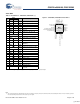
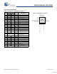

CapSense™ Applications
CY8C20x36/46/66, CY8C20396
Cypress Semiconductor Corporation • 198 Champion Court • San Jose, CA 95134-1709 • 408-943-2600
Document Number: 001-12696 Rev. *D Revised March 17, 2009
Features
■ 1.71V to 5.5V Operating Range
■ Low Power CapSense™ Block
❐ Configurable Capacitive Sensing Elements
❐ Supports Combination of CapSense Buttons, Sliders,
Touchpads, Touch Screens, and Proximity Sensor
■ Powerful Harvard Architecture Processor
❐ M8C Processor Speeds Running to 24 MHz
❐ Low Power at High Speed
❐ Interrupt Controller
❐ Temperature Range: -40°C to +85°C
■ Flexible On-Chip Memory
❐ Three Program/Data Storage Size Options:
• CY8C20x36: 8K Flash / 1K SRAM
• CY8C20x46: 16K Flash / 2K SRAM
• CY8C20x66: 32K Flash / 2K SRAM
❐ 50,000 Flash Erase/Write Cycles
❐ Partial Flash Updates
❐ Flexible Protection Modes
❐ In-System Serial Programming (ISSP)
■ Full-Speed USB
❐ Available on CY8C20396 and CY8C20666 Only
❐ 12 Mbps USB 2.0 Compliant
❐ Eight Unidirectional Endpoints
❐ One Bidirectional Control Endpoint
❐ Dedicated 512 Byte Buffer
❐ Internally Regulated at 3.3V
■ Precision, Programmable Clocking
❐ Internal Main Oscillator: 6/12/24 MHz ± 5%
❐ Internal Low Speed Oscillator at 32 kHz for Watchdog and
Sleep Timers
❐ Precision 32 kHz Oscillator for Optional External Crystal
(CY8C20x46/66 only)
❐ 0.25% Accuracy for USB with No External Components
(CY8C20396 and CY8C20666 only)
■ Programmable Pin Configurations
❐ Up to 36 GPIO (Depending on Package)
❐ Dual Mode GPIO: All GPIO Support Digital IO and Analog
Input
❐ 25 mA Sink Current on All GPIO
❐ Pull up, High Z, Open Drain Modes on All GPIO
❐ CMOS Drive Mode(5 mA Source Current) on Ports 0 and 1:
• 20 mA (at 3.0V) Total Source Current on Port 0
• 20 mA (at 3.0V) Total Source Current on Port 1
❐ Selectable, Regulated Digital IO on Port 1
❐ Configurable Input Threshold on Port 1
❐ Hot Swap Capability on all Port 1 GPIO
■ Versatile Analog Mux
❐ Common Internal Analog Bus
❐ Simultaneous Connection of IO
❐ High PSRR Comparator
❐ Low Dropout Voltage Regulator for All Analog Resources
■ Additional System Resources
❐ I
2
C™ Slave:
• Selectable to 50 kHz, 100 kHz, or 400 kHz
• No Clock Stretching Required (under most conditions)
• Implementation During Sleep Modes with Less Than
100 µA
• Hardware Address Validation
❐ SPI™ Master and Slave: Configurable 46.9 kHz - 12 MHz
❐ Three 16-Bit Timers
❐ Watchdog and Sleep Timers
❐ Internal Voltage Reference
❐ Integrated Supervisory Circuit
■ Complete Development Tools
❐ Free Development Tool (PSoC Designer™)
❐ Full Featured, In-Circuit Emulator and Programmer
❐ Full Speed Emulation
❐ Complex Breakpoint Structure
❐ 128K Trace Memory
■ Package Options
❐ CY8C20x36:
• 16-Pin 3 x 3 x 0.6 mm QFN
• 24-Pin 4 x 4 x 0.6 mm QFN
• 32-Pin 5 x 5 x 0.6 mm QFN
❐ CY8C20x46:
• 16-Pin 3 x 3 x 0.6 mm QFN
• 24-Pin 4 x 4 x 0.6 mm QFN
• 32-Pin 5 x 5 x 0.6 mm QFN
❐ CY8C20396: 24-Pin 4 x 4 x 0.6 mm QFN
❐ CY8C20x66:
• 32-Pin 5 x 5 x 0.6 mm QFN
• 48-Pin 7 x 7 x 1.0 mm QFN (with USB)
• 48-Pin SSOP
[+] Feedback