Getting Started with CapSense® Document No. 001-64846 Rev.*I Cypress Semiconductor 198 Champion Court San Jose, CA 95134-1709 Phone (USA): 800.858.1810 Phone (Intnl): 408.943.2600 http://www.cypress.
Copyrights Copyrights © Cypress Semiconductor Corporation, 2010-2013. The information contained herein is subject to change without notice. Cypress Semiconductor Corporation assumes no responsibility for the use of any circuitry other than circuitry embodied in a Cypress product. Nor does it convey or imply any license under patent or other rights.
Contents 1. Introduction.................................................................................................................................................................... 6 1.1 1.2 1.3 1.4 2. How to Use This Guide .......................................................................................................................................... 6 Cypress‘s CapSense Documentation Ecosystem ............................................................................................
2.8 2.9 3. Design Considerations ............................................................................................................................................... 33 3.1 3.2 3.3 3.4 3.5 3.6 3.7 4 Water Tolerance .................................................................................................................................................. 31 CapSense System Overview ......................................................................................................
4. CapSense Product Portfolio ....................................................................................................................................... 57 4.1 5. CapSense Selector Guide ........................................................................................................................................... 59 5.1 6. Selecting the Right CapSense Device .................................................................................................................
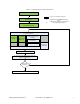
1. Introduction 1.1 How to Use This Guide ® This guide is an ideal starting point for those new to capacitive touch sensing (CapSense ) as well as for learning key design considerations and layout best practices to ensure design success.
Figure 1-1. Typical CapSense Product Design Flow 1. Capacitive touch sensing basics = Topics covered in this document 2. Specify system requirements and characteristics * † = Applicable for CY80MBR2xxx family of devices = Applicable for CapSense and CapSense Plus programmable devices 3. CapSense device selection based on needed functionality Design for CapSense 4. Mechanical design 6. PSoC Designer project creation† 5. Schematic capture and PCB layout 7. Firmware development† 8.
Table 1-1. Cypress Documents Supporting Numbered Design Tasks of Figure 1-1 Figure 1-1 Task No.
1.4 Document Conventions Convention Usage Courier New Displays file locations, user entered text, and source code: C:\ ...cd\icc\ Italics Displays file names and reference documentation: Read about the sourcefile.hex file in the PSoC Designer User Guide.
2. CapSense Technology Cypress‘s CapSense controllers use changes in capacitance to detect the presence of a finger on or near a touch surface, as shown in Figure 2-1. This touch button example illustrates a capacitive sensor replacing a mechanical button. The sensing function is achieved using a combination of hardware and firmware. The following section provides an overview of capacitive sensing technology and CapSense solutions. Figure 2-1. Illustration of a Capacitance Sensor Application 2.
2.1.2 Mutual-Capacitance Mutual-capacitance uses a pair of pins and measures the capacitance between those pins. A mutual-capacitance system operates by driving a current on a transmit pin and measuring the charge on a receive pin. When a finger is placed between the transmit and receive pins, it decreases the measured capacitance. The mutual-capacitance effect is best suited to multitouch systems, such as touchscreens and trackpads.
Figure 2-4. CapSense System Equivalent Model With a finger on the sensor surface, CX equals the sum of CP and CF. Equation 2 2.3 CapSense Sensing Technology 2.3.1 Sensing Methods There are a number of capacitive sensing methods currently in use across the electronics industry. Some of them include: Charge Transfer: The change in sensor capacitance introduced by a finger touch results in the change in charge transfer between the sensor capacitor and the reference capacitor.
Figure 2-5. Sensing Algorithm Output 2.3.3 CapSense with Sigma Delta Modulator (CSD) Cypress‘s CSD method uses a switched capacitor circuit on the front end of the system to convert the sensor capacitance to an equivalent resistor. A Sigma-Delta modulator converts the current measured through the equivalent resistor into a digital count. When a finger is on the sensor, the capacitance increases and the equivalent resistance +decreases.
The CY8C20xx6A/AS/H family of CapSense controllers uses a single external component CMOD and a single dedicated pin. Figure 2-7. CY8C20xx6A/AS/H CSD Block Diagram CY8C20x34/ CY8C20xx6A/AS/H Vref iDAC Sw2 Rbus ISENSOR Cx IDAC Gnd High-Z input Single Slope ADC AMUX Sw1 IDIFF Precharge Clock Cint(1.2nF) = External Connection 2.3.
Figure 2-8. CSA_EMC Block Diagram CY8C20x34 Vref Gnd iDAC AMUX Bus Sw2 Rbus High-Z input Single Slope ADC isensor Cx Sw1 idiff Precharge Clock Cmod = External Connection For a detailed discussion of Cypress‘s CSD and CSA_EMC sensing methods, see the respective device design guides. Table 5-1 shows the CapSense controller offerings and the sensing method supported for each. Table 5-2 compares these two CapSense sensing technologies in detail. 2.
2.4.2 Signal-to-Noise Ratio (SNR) Signal is a generic engineering term that can have many meanings. For the capacitive sensor application under consideration for CapSense applications, signal is defined as the change in the average sensor output between the OFF and ON states when the rising edge of the difference count starts below the noise threshold. Noise is another term that has many meanings.
measurement. The difference count should not be used in the measurement of SNR since it is a function of the baseline update process, which involves filtering (filling the "bucket") and nonlinear threshold events. Another factor to consider is how the signal is produced. The worst-case ON and OFF scenario should be used when measuring SNR. If the system is designed to sense the presence of a finger, then measure SNR with a light touch of the sensor area, and position the contact point slightly off-center.
Figure 2-10. Different Noise Levels in Design A and B Being Compensated Automatically 2.4.4.3.2 Noise Spikes during Production SmartSense technology also automatically tunes out the noise spikes (in production) that may not be seen during the design stage, as indicated in Figure 2-11. Noise spikes is a powerful feature prevents false button presses in the end system, which prevents a failure analysis for a mass production design. Figure 2-11.
product. SmartSense_EMC with superior noise immunity is well suited and useful for such applications to pass radiated and conducted noise tests. 2.5 Sensor Types Capacitive sensors can be broadly classified into four categories: buttons, sliders, touchscreens / trackpad, and proximity sensors. Different sensor types cater to different market segments. Figure 2-12.
2.5.1.2 Matrix Buttons In applications requiring a high number of buttons such as a calculator keypad or a QWERTY keyboard, capacitive sensors can be arranged in a matrix. This allows a design to have more buttons than there are I/O pins on the CapSense controller. Figure 2-14. Typical Matrix Buttons A matrix button design consists of two groups of capacitive sensors: Row sensors and Column sensors.
Figure 2-15. Linear Slider 2.5.2.2 Diplexed Sliders In a diplexed slider, each CapSense controller I/O pin is connected to two different slider segments. This allows a design to have twice as many slider segments as there are I/O pins. For example, a diplexed 16-segment slider requires only eight CapSense controller I/O pins. Figure 2-16. 16-Segment Diplexed Slider For a diplexed slider to work properly, the slider segments must be connected to the CapSense controller I/O pins in a pre-determined order.
2.5.2.3 Radial Sliders Radial sliders are similar to linear sliders in that finger position is estimated using data from adjacent sensors; however, radial sliders are continuous (does not have a beginning or end). Figure 2-17. Radial Slider Area contacted by finger 2.5.3 Touchscreens and Trackpads (Two-Dimensional Sensors) Cypress‘s TrueTouch touchscreen solutions use mutual capacitance sensing. For more information on these products, see TrueTouch Touchscreen Controllers.
2.6 Sensor Construction 2.6.1 Field Coupled via Copper Trace (PCB) Figure 2-19.
Features of a design based on springs/gaskets/foam: Electrical field coupled from PCB to overlay using a compressed spring, or conductive gasket or foam Conductive material itself acts as capacitive sensor pad No mechanical moving parts.
Figure 2-21. LED Sourcing and Sinking Configuration VDD R Vsrc CapSense Controller Vsnk CapSense Controller LED R CapSense button LED CapSense button Vsnk Vsrc VDD VDD ON OFF ON OFF t ON LED in Sourcing Mode OFF ON OFF t LED in Sinking mode 2.7.1.1.2 Advanced LED Effects For user interfaces that require sophisticated visual effects, a single hardware PWM or timer can be used to drive the LEDs.
2.7.1.1.4 LED Fading By gradually changing the duty cycle between LED states, you can achieve a fading effect (see Figure 2-23). For example, the LED appears to ―fade in‖ (from OFF to ON) when the duty cycle is increased in a series of small steps. Figure 2-23. LED Fading LED 100% t 2.7.1.1.5 LED Breathing Gradually increasing and decreasing the duty cycle between two levels on a continuous basis makes the LED appear to ―breathe‖, as shown in Figure 2-24.
The linear brightness levels are transferred to exponential duty cycle values using the lookup table. The following expression is used for the conversion: Equation 9 Equation 10 Figure 2-26 illustrates the table graphs at different values of parameter b. Note that NMAX is set to 255. This expression converts an 8-bit unsigned byte value to the same range. The figure shows that the transfer characteristic becomes more exponential as the b parameter increases. Figure 2-26.
Figure 2-28. Implementing LCD Feedback with CapSense on CapSense Plus 2.7.2 Haptic Feedback Haptic, or tactile, feedback uses vibration to let you know that the system has detected a finger touch. Figure 2-29. Cypress Haptics Ecosystem Vibrations are created by an actuator (DC motor) with eccentric rotating mass (ERM). When the end user touches a CapSense button, a touch signal is sent to the CapSense controller.
2.7.3 Audible Feedback Audible feedback for CapSense buttons is implemented using a buzzer. The pulse-width modulator (PWM) is used to output the PWM signal required for driving the buzzer as specified in the buzzer datasheet. The PWM user module available in PSoC is used for this purpose. PSoC can implement CapSense through its CSA and CSD algorithms. The CSD user module is configured to scan a set of buttons and sliders.
Rearranging the equation gives the following result: Equation 13 The previous equation has various integral solutions. For simplicity, this example uses N1 = 4 and N2 = 10. Substituting these values in the previous equation generates the values: Equation 14 Thus, Period Value is 249. To have a 50-percent duty cycle, the Compare value for the PWM is set as: Equation 15 User module parameters are matched as shown in the following table. Table 2-1.
2.8 Water Tolerance Capacitive touch sensing is effective in applications where the touch sensing zone is exposed to moisture, rain, or water drops. Such applications include automotive applications, outdoor equipment, ATMs, public access systems, and portable devices such as cell phones, PDAs, and kitchen and bathroom applications. Two common triggers are water droplets on sensors and the flow of water on the PCB.
Figure 2-33. Two-Layer Stack-up of a CapSense Board Four-layer designs are an option when board area must be minimized. PCB layout plays a very important role in CapSense system performance. Best practices are discussed in Design Considerations. 2.9.2 Firmware Component Firmware is a vital component of the CapSense system that processes the raw count data and makes logical decisions.
3. Design Considerations When designing capacitive touch sense technology into your application, it is important to remember that the CapSense device exists within a larger framework. Careful attention to every level of detail from PCB layout to user interface to end-use operating environment will enable robust and reliable system performance. 3.1 Overlay Selection In a CapSense design, overlay material is placed over the sensor pad to protect it from the environment and prevent direct finger contact. 3.
3.1.2 Overlay Thickness Sensitivity is inversely proportional to overlay thickness, as illustrated in Figure 3-1. Figure 3-1. Sensitivity vs. Overlay Thickness Both signal and noise are affected by the overlay properties. Table 3-2 lists the recommended maximum overlay thicknesses for PSoC CapSense applications with an acrylic overlay material. Table 3-2. Maximum Overlay Thickness with an Acrylic Overlay Material Design Element Max. Overlay Thickness (mm) Button 5 Slider 2 Touchpad 0.5 3.1.
Table 3-3. Overlay Material Dielectric Strength Material Breakdown Voltage (V/mm) Min. Overlay Thickness at 12 kV (mm) 1200–2800 10 3900 3 Air Wood – dry Glass – common 7900 1.5 13,000 0.9 PMMA Plastic (Plexiglas ) 13,000 0.9 ABS 16,000 0.8 Polycarbonate (Lexan ) 16,000 0.8 Formica 18,000 0.7 28,000 0.4 PET Film (Mylar ) 280,000 0.04 Polymide film (Kapton®) 290,000 0.04 Glass – Borosilicate (Pyrex®) ® ® FR-4 ® CapSense controller pins can withstand a direct 2-kV event.
3.2.2 Redirect If your product is densely packed, it may not be possible to prevent the discharge event. In this case, you can protect the CapSense controller by controlling where the discharge occurs. This can be achieved through a combination of PCB layout, mechanical layout of the system, and conductive tape or other shielding material. A standard practice is to place a guard ring on the perimeter of the circuit board. The guard ring should connect to chassis ground. Figure 3-3.
3.3 Electromagnetic Compatibility (EMC) Considerations EMC is related to the generation, transmission, and reception of electromagnetic energy that can upset the working of an electronic system. The source (emitter) produces the emission and a transfer or coupling path transfers the emission energy to a receptor, where it is processed, resulting in either desired or undesired behavior.
ground flood is not recommended within 1 cm of CapSense sensors or traces due to an increase in the parasitic capacitance. Figure 3-6 shows an example of an improper grounding scheme. The layout greatly improves by reducing the loop area. Figure 3-6. Improper Ground Scheme and Ground Loop 2) Each output (and input) drives the AC voltage out onto the PCB. Each signal will have a loop area associated with it.
Figure 3-8. Proper Current Loop Layout CONNECTED PATH TO SENSOR PAD RETURN PATH CapSense Sensor CapSense mC GROUND FILL OTHER CIRCUITRY PCB 3.3.1.5 RF Source Location When systems, such as computer monitors or digital photo frames, are designed with CapSense devices, make sure you prevent noise from LCD inverters and switched-mode power supplies (SMPS) from upsetting the CapSense system.
Figure 3-10. Impact of Slew Rate on Emissions The CapSense sensing methods use a switched capacitor front end to interact with the sensors. Selecting a lowfrequency for the switched-capacitor clock helps you to reduce the radiated noise from the CapSense sensor. 3.3.3 Conducted Immunity and Emissions The noise current generated by high-frequency switching circuits entering the system through the power and communication lines is called conducted noise. 3.3.3.
3.4 Software Filtering Software filters are one of the techniques of dealing with high levels of system noise. Table 3-5 lists the types of filters that are useful for CapSense. Table 3-5.
Figure 3-13. Average Filter Noise (16 Samples) Unfiltered Filtered Unfiltered Filtered Figure 3-14. Average Filter Finger Touch (16 Samples) The previous examples are representative of power supply noise. The filter works well in this example because the period of the noise is close to the length of the filter (N = 16). For more information about how to implement an average filter, see the code example CSA Software Filters with EzI2Cs Slave on CY8C20xx6. 3.4.
Figure 3-15. IIR Filter Step Response The general equation for a first-order IIR filter is: – Equation 18 Figure 3-16 and Figure 3-17 illustrate the results of a first-order IIR filter on real CapSense data using the filter equation with k = 16: Equation 19 Figure 3-16. IIR Filter Noise Getting Started with CapSense ® Document No. 001-64846 Rev.
Figure 3-17. IIR Filter Finger Touch Unfiltered Filtered Unfiltered Filtered For more information about how to implement an IIR filter, see the code example CSA Software Filters with EzI2Cs Slave on CY8C20xx6. 3.4.3 Median Filter Median filters eliminate noise spikes most commonly associated with motors and switching power supplies. In a median filter, a buffer of size N stores the N most recent samples of the input. The median is then computed using a two-step process.
Figure 3-19. Median Filter (16-sample) Finger Touch For more information about how to implement a median filter, see the code example CSA Software Filters with EzI2Cs Slave on CY8C20xx6. 3.4.4 Jitter Filter 3.4.4.1 Jitter Filter for Noisy Slider Data The centroid function is used to estimate finger position on a slider.
Figure 3-20. Jitter Filter Applied to Noisy Centroid Data Unfiltered Filtered 3.4.4.2 Jitter Filter for Raw Counts Although the jitter filter is intended for use with noisy slider data, it is also used with noisy buttons. If the change in the current input exceeds a set threshold level, the output is changed to the previous input plus or minus the threshold amount. The output is not changed if the current input changes by less than the threshold amount.
Figure 3-22. Jitter Filter for Button Finger Touch Unfiltered Filtered Unfiltered Filtered For more information about how to implement a jitter filter, see the code example CSA Software Filters with EzI2Cs Slave on CY8C20xx6. 3.4.5 Event-Based Filters Event-based filters involve a special filtering method where a pattern observed in the sensor data causes a predefined response in the CapSense system.
active state (scan all sensors, update all baselines, check if any sensor is in the TOUCH state, and so on), and then returns to sleep state. The resulting instantaneous current graph is shown in Figure 3-23. Figure 3-23.
Figure 3-24. Recommended: Port Isolation for Communication, CapSense, and LEDs The CapSense controller architecture imposes a restriction on current budget for even and odd port pin numbers. For a CapSense controller, if the current budget of an odd port pin is 100 mA, the total current drawn though all odd port pins should not exceed 100 mA. In addition to the total current budget limitation, there is also a maximum current limitation for each port pin.
The example in Figure 3-26 achieves good isolation, but it has a bad pin assignment because the LEDs are placed next to the ground pin. The CapSense sensors are assigned to the side of the chip that does not include ground. If the CapSense pins are away from the ground pin, the impedance of the ground path increases, which in turn causes the drive circuit‘s reference voltage to shift. This shift may lead to false triggering of sensors.
3.7 PCB Layout Guidelines In the typical CapSense application, the capacitive sensors are formed by the traces of a printed circuit board (PCB) or flex circuit. Following CapSense layout best practices will help your design achieve higher noise immunity, lower CP, and higher signal-to-noise ratio (SNR). The CapSense signal drops off at high CP levels due to drive limits of the internal current sources that are part of the CapSense circuitry.
Button diameter can range from 5 mm to 15 mm, with 10 mm being suitable for the majority of applications. A larger diameter helps with thicker overlays. Annular gap size should be equal to the overlay thickness, but no smaller than 0.5 mm, and no larger than 2 mm. For example, a PCB layout for a system with a 1-mm overlay should have a 1-mm annular gap, while a 3-mm overlay design should have a 2-mm annular gap.
3.7.8 Trace Routing Route sensor traces on the bottom layer of the PCB, so that the only user interaction with the CapSense sensors is with the active sensing area. Do not route traces directly under any sensor pad unless the trace is connected to that sensor. 2 Do not run capacitive sensing traces in close proximity to communication lines, such as I C or SPI masters.
Another approach to reducing crosstalk is to slow down the rising and falling edges of the LED drive voltage using a filter capacitor. Figure 3-34 shows an example circuit of this solution. The value of the added capacitor depends on the drive current requirements of the LED; however, a value of 0.1 µF is typical. Figure 3-34. Filter Capacitor Solution for Crosstalk VDD CapSense Sensor LED Sensor Port Pin CapSense Controller LED Port Pin Series resistor Capacitor 3.7.
Figure 3-37. Recommended Button and Slider Layout Bottom Layer 3.7.
Slow the edges of the shield waveform Reduce the slew rate of shield electrode by adding a filter capacitor between the shield electrode port pin and ground. Guard Sensor: The guard sensor is a copper trace that surrounds all of the buttons, as shown in Figure 3-39. Figure 3-39.
4. CapSense Product Portfolio ® Cypress‘s CapSense controller solutions are based on our Programmable System-on-Chip (PSoC ) platform and offer a wide range of features. 4.1 Cypress’s CapSense Controller Solutions Cypress is the world leader in capacitive sensing technologies and their broad range of solutions provides robust noise immunity, enable quick time to market, and system scalability. With CapSense controllers, you can: Replace mechanical components with simple CapSense buttons and sliders.
4.1.3 CapSense Plus (Programmable Solutions) Figure 4-1. CapSense Plus System Functionality ADC, Comparators, Noise Filtering 2 I C, TX8, UART, SPI, USB LED Effects, Proximity, Audio, Haptics PWM, Counters, Timers CapSense CapSense Plus CapSense Plus devices feature capacitive touch sensing and additional system functionality. Using CapSense Plus devices can result in significant cost savings.
5. CapSense Selector Guide 5.1 Selecting the Right CapSense Device Several key system requirements must be considered when selecting the best CapSense device for your application.
Figure 5-1.
Table 5-1. CapSense Sensing Method by Product Family CapSense User Modules Product Family CY8CMBR2044 CY8C201xx CY8C21x34/B CY8C20x34 CY8C20xx6A/H CY8C20xx6AS CY8C24x94 CSD Yes CSA_EMC Yes Yes SmartSense Yes Yes Yes (B) Yes Yes Yes Yes Yes Yes SmartSense_EMC Yes Yes Table 5-2.
Product Family CY8CMBR2044 CY8C201xx CY8C21x34/B CY8C20x34 CY8C20xx6A/H CY8C20xx6AS CY8C24x94 Haptics Feedback Comparators Yes Yes 8- and 10-bit ADC Yes Yes 8- and 10-bit 8- and 10-bit 7- to 13-bit 6,8 and 9-bit DAC Random Sequencer 8- to 32-bit pseudo Amplifiers Yes 2-pole band and low pass Filter Table 5-3.
6. CapSense Migration Paths As a system evolves, it may require a CapSense controller with more advanced features. The following sections describe possible migrations among CapSense controllers. 6.1 CY8C20x34 to CY8C20xx6A/H/AS CY8C20xx6A/H/AS devices implement CSA_EMC using dedicated hardware similar to that in CY8C20x34. Therefore, upgrading your design from CY8C20x34 to CY8C20xx6A/AS does not require any external hardware or firmware changes, simply clone your PSoC Designer project to CY8C20xx6A/AS.
6.4 Pin-to-Pin Compatibility When migrating from one device to another, PCB change is not required if you assign the same pin functionality to the new device. If this is the case, then the two devices are pin-to-pin compatible. Table 6-1 gives information about available device packages and pin-to-pin compatibility between the same packages of CY8C20x34, CY8C21x34/B, CY8C20xx6A/AS, and CY8C24x94 devices. Table 6-1.
7. Resources 7.1 Website At the Cypress CapSense Controllers website, you can access all the reference material discussed in this section as well as device specific datasheets and design guides. 7.2 Device Specific Design Guides Design guides are available for each CapSense family of devices. These documents are intended for design engineers who are familiar with capacitive sensing technology and have selected a family of devices.
Note CY3280-20x34 Universal CapSense Controller and CY3280-21x34 Universal CapSense Controller kits are available only as a part of the CY3280-BK1 Universal CapSense Controller - Basic Kit 1. 7.4.2 Universal CapSense Module Boards 7.4.2.1 Simple Button Module Board The CY3280-BSM Simple Button Module consists of ten CapSense buttons and ten LEDs. This module connects to any CY3280 Universal CapSense Controller Board. 7.4.2.
7.4.6 In-Circuit Emulation (ICE) Kits The ICE pod provides the interconnection between the CY3215-DK In-Circuit Emulator via a flex cable and the target PSoC device in a prototype system or PCB via package-specific pod feet. The kit guide and quick start guide for the In-Circuit Emulator (ICE) Development Kit are available here. Following are the pods available.
Figure 7-1. PSoC Designer Device Editor 7.7 PSoC Programmer PSoC Programmer is a flexible, integrated programming application to program PSoC devices. PSoC Programmer can be used with PSoC Designer and PSoC Creator to program any design on to a PSoC device. Figure 7-2. PSoC Programmer PSoC Programmer provides you a hardware layer with APIs to design specific applications using the programmers and bridge devices.
7.8 I2C-to-USB Bridge Kit 2 The CY3240-I2USB kit allows you to test, tune, and debug hardware and software by bridging the USB port to I C.
Figure 7-4. MultiChart User Interface 70 Document No. 001-64846 Rev.
7.10 Design Support Cypress has several support channels to ensure the success of your CapSense design. Code Examples – Our vast collection of code examples will help get your design up and running fast. Knowledge Base Articles – Browse technical articles by product family or perform a search on various CapSense topics. White Papers and Technical Articles – Learn about advanced capacitive touch interface topics.
8. Appendix 8.1 Appendix A: Springs 8.1.1 Finger-Introduced Capacitance This section gives the influence of various physical parameters on finger-introduced capacitance in a CapSense design with springs. Influence of overlay thickness on Finger Touch added Capacitance (FTC) with springs is similar to that with solid sensors Figure 8-1.
Influence of diameter on FTC Figure 8-3. FTC versus Spring Diameter Introduced Capacitance, pF 3 2,5 2 1,5 1 0,5 0 0 5 10 15 20 Diameter of the Spring, mm 25 Influence of wire thickness of the spring on FTC Figure 8-4. FTC versus Wire Thickness of Spring Introduced Capacitance, pF 0,59 0,58 0,57 0,56 0,55 0,54 0,53 0,52 0 1 2 3 4 Wire Thickness of the Spring, mm 5 6 8.1.2 Mounting Springs to the PCB Figure 8-5 shows an example of spring mounting.
Figure 8-6 shows examples of footprints for springs. Do not place solid grounds under the springs as this complicates the spring soldering and increases the native capacitance of the sensors. Figure 8-6. Proposed Spring Footprints PCB Trace to PSoC Spring Contour Solder points 8.1.3 CapSense and Mechanical Button Combination The hollow space inside a spring can also be used as a mechanical button, as shown in Figure 8-7. Figure 8-7.
8.2 Document Revision History Revision Issue Date Origin of Change Description of Change ** 12/17/2010 SSHH New guide *A 03/04/2011 SSHH Multiple chapter enhancements for content and reader clarity *B 08/16/2011 SSHH/BVI Multiple section and table updates *C 12/07/2011 SSHH Multiple chapter enhancements for content clarity *D 04/27/2012 UDYG Updated slider section. Updated PCB layout guidelines. Updated table 5-2. Corrected phone number in the title page.