
User guide


Getting Started with CapSense
®
Document No. 001-64846 Rev. *I 39
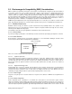
Figure 3-8. Proper Current Loop Layout
CapSense
Sensor
CapSense
mC
GROUND
FILL
CONNECTED
PATH TO
SENSOR PAD
RETURN
PATH
PCB
OTHER
CIRCUITRY
3.3.1.5 RF Source Location
When systems, such as computer monitors or digital photo frames, are designed with CapSense devices, make sure
you prevent noise from LCD inverters and switched-mode power supplies (SMPS) from upsetting the CapSense
system. A simple technique to minimize this kind of interaction is to partition the system with noise sources from
CapSense inputs, as demonstrated in Figure 3-9. Due to the practical limitations of product size, the noise source
and the CapSense circuitry may only be separated by a few inches. This small separation can provide the extra
margin required for good sensor performance compared to the case with close proximity between noise source and
CapSense.
Figure 3-9. Separating Noise Sources
Computer monitor
SMPS/LCD Inverter
CapSense interface
Computer monitor
SMPS/LCD Inverter
CapSense interface
Not Recommended Recommended
3.3.2 Radiated Emissions
Figure 3-10 shows the impact of rise/fall time of a square wave on the radiated emissions. Note that slowing the
transitions introduces the cutoff point and damps the radiated energy level. The internal clock signals of the
CapSense controller are slew-controlled to reduce the radiated emission.