
Specifications

104 CY8CKIT-042 PSoC 4 Pioneer Kit Guide, Doc. # 001-86371 Rev. *D
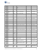
A.2 Pin Assignment Table
This section provides the pin map of the headers and their usage.
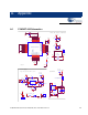
A.2.1 Arduino Compatible Headers (J1, J2, J3, J4, and J12)
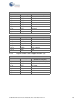
J1
Pin Kit Signal Description
J1_01 VIN Input voltage to the board
J1_02 GND GND
J1_03 GND GND
J1_04 5V 5 V voltage
J1_05 3.3V 3.3 V voltage
J1_06 RESET /XRES
J1_07 IOREF I/O voltage reference
J1_08 NC Not connected
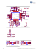
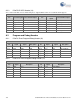
J2
Pin PSoC 4 Signal PSoC 4 Description Pin PSoC 4 Signal PSoC 4 Description
J2_01 P2[0] A0 (SARADC input) J2_02 P0[2] Comparator 2+
J2_03 P2[1] A1 (SARADC input) J2_04 P0[3] Comparator 2–
J2_05 P2[2] A2 (SARADC input) J2_06 VDD VDD
J2_07 P2[3] A3 (SARADC input) J2_08 P1[5] Opamp 2+
J2_09 P2[4] A4 (SARADC input) J2_10 P1[4] Opamp 2–
J2_11 P2[5] A5 (SARADC input) J2_12 P1[3] Opamp 2out
J2_13 P0[0] Comparator 1+ J2_14 GND GND
J2_15 P0[1] Comparator 1– J2_16 P1[2] Opamp 1out
J2_17 P1[0] Opamp 1+ J2_18 P1[1] Opamp 1–
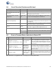
J3
Pin PSoC 4 Signal PSoC 4 Description
J3_01 P2[6] D8
J3_02 P3[6] D9(PWM)
J3_03 P3[4] D10(PWM/SS)
J3_04 P3[0] D11(PWM/MOSI)
J3_05 P3[1] D12(MISO)
J3_06 P0[6] D13(SCK)
J3_07 GND GND
J3_08 P1[7] AREF
J3_09 P4[1] SDA
J3_10 P4[0] SCL