
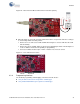
Specifications

CY8CKIT-042 PSoC 4 Pioneer Kit Guide, Doc. # 001-86371 Rev. *D 33
Hardware
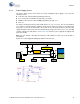
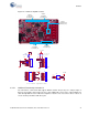
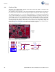
4.3.3 Power Supply System
The power supply system on this board is versatile, allowing the input supply to come from the
following sources:
■ 5-V power from onboard USB programming header J10
■ 5-V to 12-V power from Arduino shield using J1_01 header
■ VTARG - power from the onboard SWD programming using J6 or J7
■ VIN - J11
The PSoC 4 and PSoC 5LP are powered with either a 3.3 V or 5 V source. The selection between
3.3 V and 5 V is made through the J9 jumper. The board can supply 3.3 V and 5 V to the I/O headers
and receive 3.3 V from the I/O headers. The board can also be powered with an external power
supply through the VIN (J11) header; the allowed voltage range for the VIN is 5 V to 12 V. The LDO
regulator regulates the VIN down to 3.3 V. Figure 4-4 shows the power supply block diagram and
protection circuitry.
Note: The 5-V domain is directly powered by the USB (VBUS). For this reason, this domain is
unregulated.
Figure 4-4. Power Supply Block Diagram with Protection Circuits
I/OHeader
USB
5V
Vin
3.3V
PSoC5LP
USB
5V
P4 10pin
Debug
P5LP I/O
Header
PTC
LDO
D1
D2
D3
D4
ESD
Protection
J9
P5LP 10pin
Debug
MOSFETbased
ProtectionCkt
PSoC4