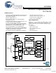
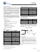
CY7C67200 EZ-OTG™ Programmable USB On-The-Go EZ-OTG Features • Single-chip programmable USB dual-role (Host/Peripheral) controller with two configurable Serial Interface Engines (SIEs) and two USB ports • Supports USB OTG protocol • On-chip 48-MHz 16-bit processor with dynamically switchable clock speed • Configurable IO block supports a variety of IO options or up to 25 bits of General Purpose IO (GPIO) • 4K × 16 internal mask ROM contains built-in BIOS that supports a communication-ready state with acces
CY7C67200 Introduction Interrupts EZ-OTG™ (CY7C67200) is Cypress Semiconductor’s first USB On-The-Go (OTG) host/peripheral controller. EZ-OTG is designed to easily interface to most high-performance CPUs to add USB host functionality. EZ-OTG has its own 16-bit RISC processor to act as a coprocessor or operate in standalone mode. EZ-OTG also has a programmable IO interface block allowing a wide range of interface options. EZ-OTG provides 128 interrupt vectors.
CY7C67200 USB Interface OTG Interface EZ-OTG has two built-in Host/Peripheral SIEs that each have a single USB transceiver, meeting the USB 2.0 specification requirements for full and low speed (high speed is not supported). In Host mode, EZ-OTG supports two downstream ports; each supports control, interrupt, bulk, and isochronous transfers. In Peripheral mode, EZ-OTG supports one peripheral port with eight endpoints for each of the two SIEs.
CY7C67200 UART Features • Supports baud rates of 900 to 115.2K • 8-N-1 • Individual bit transfer for non-byte aligned serial communication in PIO mode • Programmable delay timing for the active/inactive master SPI clock • Auto or manual control for master mode slave select signal • Complete access to internal memory UART Pins Table 5.
CY7C67200 Table 9. HPI Interface Pins [1, 2] (continued) Host Port Interface (HPI) EZ-OTG has an HPI interface. The HPI interface provides DMA access to the EZ-OTG internal memory by an external host, plus a bidirectional mailbox register for supporting high-level communication protocols. This port is designed to be the primary high-speed connection to a host processor. Complete control of EZ-OTG can be accomplished through this interface via an extensible API and communication protocol.
CY7C67200 Charge Pump Features • Meets OTG Supplement Requirements, see Table 41, “DC Characteristics: Charge Pump,” on page 66. Figure 3. Power Supply Connection Without Booster BOOSTVcc 3.0V to 3.6V Power Supply Charge Pump Pins Table 11.Charge Pump Interface Pins Pin Name Pin Number OTGVBUS C1 CSwitchA D1 CSwitchB D2 VSWITCH VCC AVCC Booster Interface EZ-OTG has an on-chip power booster circuit for use with power supplies that range between 2.7V and 3.6V.
CY7C67200 Crystal Pins Operational Modes Table 13.Crystal Pins There are two modes of operation: Coprocessor and Standalone. Pin Name Pin Number XTALIN G3 Coprocessor Mode XTALOUT G2 EZ-OTG can act as a coprocessor to an external host processor. In this mode, an external host processor drives EZ-OTG and is the main processor rather then EZ-OTG’s own 16-bit internal CPU.
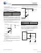
CY7C67200 Minimum Hardware Requirements for Standalone Mode – Peripheral Only Figure 5. Minimum Standalone Hardware Configuration – Peripheral Only EZ-OTG CY7C67200 VCC, AVCC, BoostVCC VReg Standard-B or Mini-B VBus D+ Reset Logic nRESET DPlus DMinus DGND SHIELD Bootstrap Options Vcc Vcc 10k 10k GPIO[30] SCL* GPIO[31] SDA* Int.
CY7C67200 External (Remote) Wakeup Source There are several possible events available to wake EZ-OTG from Sleep mode as shown in Table 15. These may also be used as remote wakeup options for USB applications. See section “Power Control Register [0xC00A] [R/W]” on page 13. Upon wakeup, code begins executing within 200 ms, the time it takes the PLL to stabilize. Table 15.
CY7C67200 Registers Table 16.Processor Control Registers Some registers have different functions for a read vs. a write access or USB host vs. USB device mode. Therefore, registers of this type have multiple definitions for the same address. Address R/W CPU Flags Register Register Name 0xC000 R Register Bank Register 0xC002 R/W The default register values listed in this data sheet may be altered to some other value during BIOS initialization.
CY7C67200 Bank Register [0xC002] [R/W] Figure 8. Bank Register Bit # 15 14 13 12 Field Read/Write 11 10 9 8 Address... R/W R/W R/W R/W R/W R/W R/W R/W Default 0 0 0 0 0 0 0 1 Bit # 7 6 5 4 3 2 1 0 Field Read/Write Default ...Address Reserved R/W R/W R/W - - - - - 0 0 0 X X X X X Register Description . Table 17.Bank Register Example The Bank register maps registers R0–R15 into RAM.
CY7C67200 CPU Speed Register [0xC008] [R/W] Figure 10. CPU Speed Register Bit # 15 14 13 12 Field 11 10 9 8 Reserved... Read/Write - - - - - - - - Default 0 0 0 0 0 0 0 0 Bit # 7 6 5 4 3 2 1 0 Field ...Reserved CPU Speed Read/Write - - - - R/W R/W R/W R/W Default 0 0 0 0 1 1 1 1 Register Description The CPU Speed register allows the processor to operate at a user selected speed.
CY7C67200 Power Control Register [0xC00A] [R/W] Figure 11.
CY7C67200 immediately following the HALT instruction may be executed before the waking interrupt is serviced (you may want to follow the HALT instruction with two NOPs). Halt Enable (Bit 0) Setting this bit to ‘1’ immediately initiates HALT mode. While in HALT mode, only the CPU is stopped. The internal clock still runs and all peripherals still operate, including the USB engines.
CY7C67200 UART Interrupt Enable (Bit 3) Timer 1 Interrupt Enable (Bit 1) The UART Interrupt Enable bit enables or disables the following UART hardware interrupts: UART TX and UART RX. 1: Enable UART interrupt The Timer 1 Interrupt Enable bit enables or disables the TImer1 Interrupt Enable. When this bit is reset, all pending Timer 1 interrupts are cleared.
CY7C67200 USB Diagnostic Register [0xC03C] [R/W] Figure 14. USB Diagnostic Register Bit # 15 14 13 12 Reserved Port 2A Diagnostic Enable Reserved Port 1A Diagnostic Enable Read/Write - R/W - R/W - - - - Default 0 0 0 0 0 0 0 0 2 1 0 Field Bit # 11 10 9 8 Reserved... 7 6 5 4 3 ...
CY7C67200 Watchdog Timer Register [0xC00C] [R/W] Figure 15. Watchdog Timer Register Bit # 15 14 13 12 Field Read/Write 11 10 9 8 Reserved... R/W R/W R/W R/W R/W R/W R/W R/W Default 0 0 0 0 0 0 0 0 Bit # 7 5 4 6 ...
CY7C67200 Timer n Register [R/W] • Timer 0 Register 0xC010 • Timer 1 Register 0xC012 Figure 16. Timer n Register Bit # 15 14 13 12 Field 11 10 9 8 Count... Read/Write R/W R/W R/W R/W R/W R/W R/W R/W Default 1 1 1 1 1 1 1 1 Bit # 7 6 5 4 3 2 1 0 Field ...Count Read/Write Default R/W R/W R/W R/W R/W R/W R/W R/W 1 1 1 1 1 1 1 1 Register Description The Timer n Register sets the Timer n count.
CY7C67200 Port A D+ Status (Bit 13) Table 24.Port A Force D± State The Port A D+ Status bit is a read-only bit that indicates the value of DATA+ on Port A. 1: D+ is high 0: D+ is low Port A D– Status (Bit 12) The Port A D– Status bit is a read-only bit that indicates the value of DATA– on Port A.
CY7C67200 Host n Control Register [R/W] • Host 1 Control Register 0xC080 • Host 2 Control Register 0xC0A0 Figure 18.
CY7C67200 Host n Address Register [R/W] • Host 1 Address Register 0xC082 • Host 2 Address Register 0xC0A2 Figure 19. Host n Address Register Bit # 15 14 13 12 Field Read/Write 11 10 9 8 Address... R/W R/W R/W R/W R/W R/W R/W R/W Default 0 0 0 0 0 0 0 0 Bit # 7 6 5 4 3 2 1 0 Field Read/Write Default ...
CY7C67200 Host n Endpoint Status Register [R] • Host 1 Endpoint Status Register 0xC086 • Host 2 Endpoint Status Register 0xC0A6 Figure 21.
CY7C67200 1: For non-Isochronous transfers, the transaction was ACKed. For Isochronous transfers, the transaction was completed successfully. ACK Flag (Bit 0) The ACK Flag bit indicates two different conditions depending on the transfer type. For non-Isochronous transfers, this bit represents a transaction ending by receiving or sending an ACK packet. For Isochronous transfers, this bit represents a successful transaction that will not be represented by an ACK packet.
CY7C67200 Host n Count Result Register [R] • Host 1 Count Result Register 0xC088 • Host 2 Count Result Register 0xC0A8 Figure 23. Host n Count Result Register Bit # 15 14 13 12 Field 11 10 9 8 Result... Read/Write R R R R R R R R Default 0 0 0 0 0 0 0 0 Bit # 7 6 5 4 3 2 1 0 Field ...
CY7C67200 Host n Interrupt Enable Register [R/W] • Host 1 Interrupt Enable Register 0xC08C • Host 2 Interrupt Enable Register 0xC0AC Figure 25.
CY7C67200 Host n Status Register [R/W] • Host 1 Status Register 0xC090 • Host 2 Status Register 0xC0B0 Figure 26.
CY7C67200 Host n SOF/EOP Count Register [R/W] • Host 1 SOF/EOP Count Register 0xC092 • Host 2 SOF/EOP Count Register 0xC0B2 Figure 27. Host n SOF/EOP Count Register Bit # 15 Field 14 13 12 11 Reserved 10 9 8 Count... Read/Write - - R/W R/W R/W R/W R/W R/W Default 0 0 1 0 1 1 1 0 Bit # 7 6 5 4 3 2 1 0 R/W R/W R/W R/W R/W R/W R/W R/W 1 1 1 0 0 0 0 0 Field Read/Write Default ...
CY7C67200 Host n Frame Register [R] • Host 1 Frame Register 0xC096 • Host 2 Frame Register 0xC0B6 Figure 29. Host n Frame Register Bit # 15 14 12 11 10 Read/Write - - - - - R Default 0 R R 0 0 0 0 0 0 0 Bit # 7 6 5 4 3 2 1 0 Read/Write R R R R R R R R Default 0 0 0 0 0 0 0 0 Field 13 Reserved 9 8 Frame... Field ...
CY7C67200 Figure 30.
CY7C67200 Device n Endpoint n Address Register [R/W] • Device n Endpoint 0 Address Register [Device 1: 0x0202 Device 2: 0x0282] • Device n Endpoint 1 Address Register [Device 1: 0x0212 Device 2: 0x0292] • Device n Endpoint 2 Address Register [Device 1: 0x0222 Device 2: 0x02A2] • Device n Endpoint 3 Address Register [Device 1: 0x0232 Device 2: 0x02B2] • Device n Endpoint 4 Address Register [Device 1: 0x0242 Device 2: 0x02C2] • Device n Endpoint 5 Address Register [Device 1: 0x0252 Device 2: 0x02D2] • Device
CY7C67200 Register Description The Device n Endpoint n Count register designates the maximum packet size that can be received from the host for OUT transfers for a single endpoint. This register also designates the packet size to be sent to the host in response to the next IN token for a single endpoint. The maximum packet length is 1023 bytes in ISO mode. There are a total of eight endpoints for each of the two ports. All endpoints have the same definition for their Device n Endpoint n Count register.
CY7C67200 IN Exception Flag (Bit 8) 1: Setup packet was received The IN Exception Flag bit indicates when the device received an IN packet when armed for an OUT. 0: Setup packet was not received 1: Received IN when armed for OUT 0: Received OUT when armed for OUT Stall Flag (Bit 7) The Stall Flag bit indicates that a Stall packet was sent to the host. Sequence Flag (Bit 3) The Sequence Flag bit indicates whether the last data toggle received was a DATA1 or a DATA0.
CY7C67200 Device n Endpoint n Count Result Register [R/W] • Device n Endpoint 0 Count Result Register [Device 1: 0x0208 Device 2: 0x0288] • Device n Endpoint 1 Count Result Register [Device 1: 0x0218 Device 2: 0x0298] • Device n Endpoint 2 Count Result Register [Device 1: 0x0228 Device 2: 0x02A8] • Device n Endpoint 3 Count Result Register [Device 1: 0x0238 Device 2: 0x02B8] • Device n Endpoint 4 Count Result Register [Device 1: 0x0248 Device 2: 0x02C8] • Device n Endpoint 5 Count Result Register [Device 1
CY7C67200 Device n Interrupt Enable Register [R/W] • Device 1 Interrupt Enable Register 0xC08C • Device 2 Interrupt Enable Register 0xC0AC Figure 35.
CY7C67200 EP5 Interrupt Enable (Bit 5) EP2 Interrupt Enable (Bit 2) The EP5 Interrupt Enable bit enables or disables an endpoint five (EP5) Transaction Done interrupt. An EPx Transaction Done interrupt triggers when any of the following responses or events occur in a transaction for the device’s given Endpoint: send/receive ACK, send STALL, Timeout occurs, IN Exception Error, or OUT Exception Error.
CY7C67200 Device n Address Register [W] • Device 1 Address Register 0xC08E • Device 2 Address Register 0xC0AE Figure 36. Device n Address Register Bit # 15 14 13 12 Read/Write - - - - - - - - Default 0 0 0 0 0 0 0 0 Bit # 7 6 5 4 3 2 1 0 Field ...Reserved Field 11 10 9 8 Reserved... Address Read/Write - W W W W W W W Default 0 0 0 0 0 0 0 0 Register Description The Device n Address register holds the device address assigned by the host.
CY7C67200 Reset Interrupt Flag (Bit 8) 0: Interrupt did not trigger The Reset Interrupt Flag bit indicates if the USB Reset Detected interrupt has triggered. EP3 Interrupt Flag (Bit 3) 1: Interrupt triggered 0: Interrupt did not trigger EP7 Interrupt Flag (Bit 7) The EP7 Interrupt Flag bit indicates if the endpoint seven (EP7) Transaction Done interrupt has triggered.
CY7C67200 Device n Frame Number Register [R] • Device 1 Frame Number Register 0xC092 • Device 2 Frame Number Register 0xC0B2 Figure 38. Device n Frame Number Register Bit # 15 Field SOF/EOP Timeout Flag 14 13 12 SOF/EOP Timeout Interrupt Counter 11 10 Reserved 9 8 Frame... Read/Write R R R R - R R R Default 0 0 0 0 0 0 0 0 Bit # 7 6 5 4 3 2 1 0 Field ...
CY7C67200 OTG Control Registers Table 28.OTG Registers There is one register dedicated for OTG operation. This register is covered in this section and summarized in Table 28. Register Name OTG Control Register Address R/W C098H R/W OTG Control Register [0xC098] [R/W] Figure 40.
CY7C67200 1: OTG VBus is greater then 4.4V 0: OTG VBus is less then 4.4V VBUS Valid Flag (Bit 0) The VBUS Valid Flag bit indicates whether OTG VBus is greater than 4.4V. After turning on VBUS, firmware should wait at least 10 µs before this reading this bit. Reserved All reserved bits must be written as ‘0’. GPIO Registers There are seven registers dedicated for GPIO operations. These seven registers are covered in this section and summarized in Table 29. Table 29.
CY7C67200 HSS Enable (Bit 7) Interrupt 0 Polarity Select (Bit 1) The HSS Enable bit routes HSS to GPIO[15:12]. The Interrupt 0 Polarity Select bit selects the polarity for IRQ0. 1: HSS is routed to GPIO 1: Sets IRQ0 to rising edge 0: HSS is not routed to GPIOs. GPIO[15:12] are free for other purposes. 0: Sets IRQ0 to falling edge SPI Enable (Bit 5) The Interrupt 0 Enable bit enables or disables IRQ0.
CY7C67200 Writing a 1 to any bit will output a high voltage on the corresponding GPIO pin. Reserved All reserved bits must be written as ‘0’. GPIO 0 Input Data Register [0xC020] [R] Figure 44.
CY7C67200 Register Description The GPIO 0 Direction register controls the direction of the GPIO data pins (input/output). The GPIO 0 Direction register controls GPIO15 to GPIO0 while the GPIO 1 Direction register controls GPIO31 to GPIO19. When any bit of this register is set to ‘1’, the corresponding GPIO data pin becomes an output. When any bit of this register is set to ‘0’, the corresponding GPIO data pin becomes an input. Reserved All reserved bits must be written as ‘0’.
CY7C67200 HSS Control Register [0xC070] [R/W] Figure 48.
CY7C67200 Transmit Ready (Bit 4) Receive Packet Ready Flag (Bit 1) The Transmit Ready bit is a read only bit that indicates if the HSS Transmit FIFO is ready for the CPU to load new data for transmission. The Receive Packet Ready Flag bit is a read only bit that indicates if the HSS receive FIFO is full with eight bytes.
CY7C67200 HSS Transmit Gap Register [0xC074] [R/W] Figure 50. HSS Transmit Gap Register Bit # 15 14 13 12 Field 11 10 9 8 Reserved Read/Write - - - - - - - - Default 0 0 0 0 0 0 0 0 Bit # 7 6 5 4 3 2 1 0 Field Read/Write Default Transmit Gap Select R/W R/W R/W R/W R/W R/W R/W R/W 0 0 0 0 1 0 0 1 Register Description The HSS Transmit Gap register is only valid in block transmit mode.
CY7C67200 HSS Receive Address Register [0xC078] [R/W] Figure 52. HSS Receive Address Register Bit # 15 14 13 12 Field Read/Write 11 10 9 8 Address... R/W R/W R/W R/W R/W R/W R/W R/W Default 0 0 0 0 0 0 0 0 Bit # 7 6 5 4 3 2 1 0 Field Read/Write ...Address R/W R/W R/W R/W R/W R/W R/W R/W 0 0 0 0 0 0 0 0 Default Register Description The HSS Receive Address register is used as the base pointer address for the next HSS block receive transfer.
CY7C67200 HSS Transmit Address Register [0xC07C] [R/W] Figure 54. HSS Transmit Address Register Bit # 15 14 13 12 Field Read/Write 11 10 9 8 Address... R/W R/W R/W R/W R/W R/W R/W R/W Default 0 0 0 0 0 0 0 0 Bit # 7 6 5 4 3 2 1 0 Field Read/Write ...Address R/W R/W R/W R/W R/W R/W R/W R/W 0 0 0 0 0 0 0 0 Default Register Description The HSS Transmit Address register is used as the base pointer address for the next HSS block transmit transfer.
CY7C67200 HPI Breakpoint Register [0x0140] [R] Figure 56. HPI Breakpoint Register Bit # 15 14 13 12 Field 11 10 9 8 Address... Read/Write R R R R R R R R Default 0 0 0 0 0 0 0 0 Bit # 7 6 5 4 3 2 1 0 Field ...Address Read/Write R R R R R R R R Default 0 0 0 0 0 0 0 0 Register Description The HPI Breakpoint register is a special on-chip memory location, which the external processor can access using normal HPI memory read/write cycles.
CY7C67200 SOF/EOP2 to CPU Enable (Bit 12) Resume2 to HPI Enable (Bit 7) The SOF/EOP2 to CPU Enable bit routes the SOF/EOP2 interrupt to the on-chip CPU. Since the SOF/EOP2 interrupt can be routed to both the on-chip CPU and the HPI port the firmware must ensure only one of the two (CPU, HPI) resets the interrupt. The Resume2 to HPI Enable bit routes the USB Resume interrupt that occurs on Host 2 to the HPI port instead of the on-chip CPU.
CY7C67200 SIEXmsg Register [W] • SIE1msg Register 0x0144 • SIE2msg Register 0x0148 Figure 58. SIEXmsg Register Bit # 15 14 13 12 Field 11 10 9 8 Data... Read/Write W W W W W W W W Default X X X X X X X X Bit # 7 6 5 4 3 2 1 0 Field ...Data Read/Write W W W W W W W W Default X X X X X X X X Register Description The SIEXmsg register allows an interrupt to be generated on the HPI port.
CY7C67200 HPI Status Port [] [HPI: R] Figure 60.
CY7C67200 mode this read only bit indicates if any of the endpoint interrupts occurs on Device 2. Firmware needs to determine which endpoint interrupt occurred. Reset1 Flag (Bit 1) 1: Interrupt triggered 1: Interrupt triggered 0: Interrupt did not trigger 0: Interrupt did not trigger Done1 Flag (Bit 2) Mailbox Out Flag (Bit 0) In host mode the Done 1 Flag bit is a read-only bit that indicates if a host packet done interrupt occurs on Host 1.
CY7C67200 3Wire Enable (Bit 15) Master Active Enable (Bit 7) The 3Wire Enable bit indicates if the MISO and MOSI data lines are tied together allowing only half duplex operation. The Master Active Enable bit is a read-only bit that indicates if the master state machine is active or idle. This field only applies to master mode.
CY7C67200 SPI Control Register [0xC0CA] [R/W] Figure 62.
CY7C67200 Receive Bit Length (Bits [2:0]) The Receive Bit Length field controls whether a full byte or partial byte will be received. If Receive Bit Length is ‘000’ then a full byte will be received. If Receive Bit Length is ‘001’ to ‘111’, then the value indicates the number of bits that will be received. SPI Interrupt Enable Register [0xC0CC] [R/W] Figure 63. SPI Interrupt Enable Register Bit # 15 14 13 12 Field 11 10 9 8 Reserved...
CY7C67200 Transmit Interrupt Flag (Bit 1) Transfer Interrupt Flag (Bit 0) The Transmit Interrupt Flag is a read only bit that indicates a byte mode transmit interrupt has triggered. The Transfer Interrupt Flag is a read only bit that indicates a block mode interrupt has triggered.
CY7C67200 CRC Enable (Bit 13) One in CRC (Bit 10) The CRC Enable bit enables or disables the CRC operation. 1: Enables CRC operation The One in CRC bit is a read-only bit that indicates if the CRC value is all zeros or not. 0: Disables CRC operation 1: CRC value is not all zeros 0: CRC value is all zeros CRC Clear (Bit 12) Zero in CRC (Bit 9) The CRC Clear bit will clear the CRC with a load of all ones. This bit is self clearing and always reads ‘0’.
CY7C67200 Data Ready bit of the SPI Control register is set to ‘1’. Writing to this register in PIO byte mode will initiate a transfer of data, the number of bits defined by Transmit Bit Length field in the SPI Control register. Data (Bits [7:0]) The Data field contains data received or to be transmitted on the SPI port. Reserved All reserved bits must be written as ‘0’. SPI Transmit Address Register [0xC0D8] [R/W] Figure 69.
CY7C67200 SPI Receive Address Register [0xC0DC [R/W] Figure 71. SPI Receive Address Register Bit # 15 14 13 12 Field Read/Write 11 10 9 8 Address... R/W R/W R/W R/W R/W R/W R/W R/W Default 0 0 0 0 0 0 0 0 Bit # 7 6 5 4 3 2 1 0 Field Read/Write Default ...Address R/W R/W R/W R/W R/W R/W R/W R/W 0 0 0 0 0 0 0 0 9 8 Register Description The SPI Receive Address register is issued as the base address for the SPI Receive DMA.
CY7C67200 UART Control Register [0xC0E0] [R/W] Figure 73. UART Control Register Bit # 15 14 13 12 11 Field 10 9 8 Reserved... Read/Write - - - - - - - - Default 0 0 0 0 0 0 0 0 Bit # 7 6 5 4 3 2 1 ...
CY7C67200 Receive Full (Bit 1) Transmit Full (Bit 0) The Receive Full bit indicates whether the receive buffer is full. It can be programmed to interrupt the CPU as interrupt #5 when the buffer is full. This can be done though the UART bit of the Interrupt Enable register (0xC00E). This bit will automatically be cleared when data is read from the UART Data register. 1: Receive buffer full The Transmit Full bit indicates whether the transmit buffer is full.
CY7C67200 Pin Diagram The following describes the CY7C67200 48-pin FBGA. Figure 76.
CY7C67200 Table 38.
CY7C67200 Table 38.Pin Descriptions (continued) Pin A6 F1 E2 E1 C1 D1 D2 G1 B1 H2, D6, A4 G6, B6, A1, H1 Name Reserved BOOSTVCC VSWITCH BOOSTGND OTGVBUS CSWITCHA CSWITCHB AVCC AGND VCC GND Type – Power Analog Output Ground Analog IO Analog Analog Power Ground Power Ground Description Tie to Gnd for normal operation. Booster Power Input: 2.7V to 3.
CY7C67200 DC Characteristics Table 40.DC Characteristics[6] Parameter Description Conditions Min. Typ. Max. Unit 3.3 3.6 V 3.6 V VCC, AVCC Supply Voltage 3.0 BoosVCC Supply Voltage 2.7 VIH Input HIGH Voltage 2.0 VIL Input LOW Voltage 5.5 V 0.8 V +10.0 µA II Input Leakage Current 0< VIN < VCC –10.0 VOH Output Voltage HIGH IOUT = 4 mA 2.
CY7C67200 Table 41.DC Characteristics: Charge Pump (continued) Parameter Description Max. Unit VA_SESS_VALID A-Device Session Valid Conditions Min. 0.8 2.0 V VB_SESS_VALID B-Device Session Valid 0.8 4.0 V VA_SESS_END B-Device Session End 0.2 0.8 V E Efficiency When Loaded RPD Data Line Pull Down RA_BUS_IN A-device VBUS Input Impedance to GND RB_SRP_UP B-device VBUS SRP Pull Up RB_SRP_DWN B-device VBUS SRP Pull Down ILOAD = 8 mA, VCC = 3.3V Typ. 75 % 14.25 24.
CY7C67200 Clock Timing tCLK tLOW XTALIN tFALL tHIGH tRISE Clock Timing Parameter Description Min. fCLK Clock Frequency vXINH[10] Clock Input High (XTALOUT left floating) tCLK Clock Period tHIGH Clock High Time 36 tLOW Clock Low Time 36 tRISE Clock Rise Time tFALL Clock Fall Time Typ. Max. Unit 12.0 Duty Cycle MHz 1.5 3.0 3.6 V 83.17 83.33 83.5 ns 44 ns 45 44 ns 5.0 ns 5.0 ns 55 % I2C EEPROM Timing 1.
CY7C67200 HPI (Host Port Interface) Write Cycle Timing tCYC tASU tWP tAH ADDR [1:0] tCSH tCSSU nCS nWR nRD Dout [15:0] tDSU Parameter tWDH Description Min. tASU Address Setup –1 Typical Max. Unit ns tAH Address Hold –1 ns tCSSU Chip Select Setup –1 ns tCSH Chip Select Hold –1 ns tDSU Data Setup 6 ns tWDH Write Data Hold 2 ns tWP Write Pulse Width 2 T[11] tCYC Write Cycle Time 6 T[11] Note 11. T = system clock period = 1/48 MHz. Document #: 38-08014 Rev.
CY7C67200 HPI (Host Port Interface) Read Cycle Timing tCYC tASU tRP tAH ADDR [1:0] tCSH tCSSU nCS tRDH nWR nRD Din [15:0] tACC Parameter tRDH Description Min.
CY7C67200 HSS BYTE Mode Transmit qt_clk CPU may start another BYTE transmit right after TxRdy goes high CPU_A[2:0] CPUHSS_cs CPU_wr BT BT TxRdy flag HSS_TxD start bit Byte transmit triggered by a CPU write to the HSS_TxData register bit 0 bit 1 bit 2 bit 3 bit 4 bit 5 bit 6 bit 7 start of last data bit to TxRdy high: 0 min, 4 T max. (T is qt_clk period) TxRdy low to start bit delay: 0 min, BT max when starting from IDEL.
CY7C67200 Hardware CTS/RTS Handshake tCTShold tCTShold tCTSsetup tCTSsetup HSS_RTS HSS_CTS HSS_TxD Start of transmission delayed until HSS_CTS goes high Start of transmission not delayed by HSS_CTS tCTSset-up: HSS_CTS setup time before HSS_RTS = 1.5T min. tCTShold: HSS_CTS hold time after START bit = 0 ns min. T = 1/48 MHz. When RTS/CTS hardware handshake is enabled, transmission can be held off by deasserting HSS_CTS at least 1.5T before HSS_RTS. Transmission resumes when HSS_CTS returns HIGH.
CY7C67200 Register Summary Table 42. Register Summary R/W R Address Register 0x0140 HPI Breakpoint Bit 15 Bit 14 Bit 13 Bit 12 Bit 11 Bit 10 Bit 9 Bit 8 Default High Bit 7 Bit 6 Bit 5 Bit 4 Bit 3 Bit 2 Bit 1 Bit 0 Default Low Address... 0000 0000 ...
CY7C67200 Table 42.
CY7C67200 Table 42.
CY7C67200 Table 42. Register Summary (continued) R/W R/W R/W Address Register 0xC0D6 0xC0D8 SPI Data Port t SPI Transmit Address Bit 15 Bit 14 Bit 13 Bit 12 Bit 11 Bit 10 Bit 9 Bit 8 Default High Bit 7 Bit 6 Bit 5 Bit 4 Bit 3 Bit 2 Bit 1 Bit 0 Default Low Reserved xxxx xxxx Data xxxx xxxx Address... 0000 0000 ...Address R/W R/W 0xC0DA 0xC0DC SPI Transmit Count SPI Receive Address 0000 0000 Reserved Count... 0000 0000 ...Count 0000 0000 Address... 0000 0000 ...
CY7C67200 Ordering Information Table 43.Ordering Information PB-Free Temperature Range CY7C67200-48BAXI Ordering Code 48FBGA Package Type X –40 to 85°C CY7C67200-BAXIT 48FBGA, Tape and reel X –40 to 85°C CY3663 Development Kit Package Diagram 48-Ball (7.00 mm x 7.00 mm x 1.2 mm) FBGA BA48 BOTTOM VIEW TOP VIEW PIN 1 CORNER Ø0.05 M C PIN 1 CORNER (LASER MARK) Ø0.25 M C A B Ø0.30±0.05(48X) 1 2 3 4 5 6 6 4 3 2 1 C F G D E F 2.625 E 0.75 C 5.25 B 7.00±0.10 A B D 7.
CY7C67200 Document History Page Document Title: CY7C67200 EZ-OTG™ Programmable USB On-The-Go Host/Peripheral Controller Document Number: 38-08014 REV. ECN NO. Issue Date Orig.