
User manual


CY7C67200
Document #: 38-08014 Rev. *G Page 13 of 78
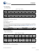
Power Control Register [0xC00A] [R/W]
Figure 11. Power Control Register
Register Description
The Power Control register controls the power-down and
wakeup options. Either the sleep mode or the halt mode
options can be selected. All other writable bits in this register
can be used as a wakeup source while in sleep mode.
Host/Device 2 Wake Enable (Bit 14)
The Host/Device 2 Wake Enable bit enables or disables a
wakeup condition to occur on an Host/Device 2 transition. This
wake up from the SIE port does not cause an interrupt to the
on-chip CPU.
1: Enable wakeup on Host/Device 2 transition.
0: Disable wakeup on Host/Device 2 transition.
Host/Device 1 Wake Enable (Bit 12)
The Host/Device 1 Wake Enable bit enables or disables a
wakeup condition to occur on an Host/Device 1 transition. This
wakeup from the SIE port does not cause an interrupt to the
on-chip CPU.
1: Enable wakeup on Host/Device 1 transition
0: Disable wakeup on Host/Device 1 transition
OTG Wake Enable (Bit 11)
The OTG Wake Enable bit enables or disables a wakeup
condition to occur on either an OTG VBUS_Valid or OTG ID
transition (IRQ20).
1: Enable wakeup on OTG VBUS valid or OTG ID transition
0: Disable wakeup on OTG VBUS valid or OTG ID transition
HSS Wake Enable (Bit 9)
The HSS Wake Enable bit enables or disables a wakeup
condition to occur on an HSS Rx serial input transition. The
processor may take several hundreds of microseconds before
being operational after wakeup. Therefore, the incoming data
byte that causes the wakeup will be discarded.
1: Enable wakeup on HSS Rx serial input transition
0: Disable wakeup on HSS Rx serial input transition
SPI Wake Enable (Bit 8)
The SPI Wake Enable bit enables or disables a wakeup
condition to occur on a falling SPI_nSS input transition. The
processor may take several hundreds of microseconds before
being operational after wakeup. Therefore, the incoming data
byte that causes the wakeup will be discarded.
1: Enable wakeup on falling SPI nSS input transition
0: Disable SPI_nSS interrupt
HPI Wake Enable (Bit 7)
The HPI Wake Enable bit enables or disables a wakeup
condition to occur on an HPI interface read.
1: Enable wakeup on HPI interface read
0: Disable wakeup on HPI interface read
GPI Wake Enable (Bit 4)
The GPI Wake Enable bit enables or disables a wakeup
condition to occur on a GPIO(25:24) transition.
1: Enable wakeup on GPIO(25:24) transition
0: Disable wakeup on GPIO(25:24) transition
Boost 3V OK (Bit 2)
The Boost 3V OK bit is a read only bit that returns the status
of the OTG Boost circuit.
1: Boost circuit not ok and internal voltage rails are below 3.0V
0: Boost circuit ok and internal voltage rails are at or above
3.0V
Sleep Enable (Bit 1)
Setting this bit to ‘1’ immediately initiates SLEEP mode. While
in SLEEP mode, the entire chip is paused achieving the lowest
standby power state. All operations are paused, the internal
clock is stopped, the booster circuit and OTG VBUS charge
pump are all powered down, and the USB transceivers are
powered down. All counters and timers are paused but will
retain their values. SLEEP mode exits by any activity selected
in this register. When SLEEP mode ends, instruction
execution resumes within 0.5 ms.
1:
Enable Sleep Mode
0: No Function
Bit # 15 14 13 12 11 10 9 8
Field
Reserved Host/Device 2
Wake Enable
Reserved Host/Device 1
Wake Enable
OTG
Wake Enable
Reserved HSS
Wake Enable
SPI
Wake Enable
Read/Write - R/W - R/W R/W - R/W R/W
Default 0 0 0 0 0 0 0 0
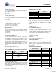
Bit # 7 6 5 4 3 2 1 0
Field
HPI
Wake Enable
Reserved GPI
Wake Enable
Reserved Boost 3V
OK
Sleep
Enable
Halt
Enable
Read/Write R/W - - R/W - R R/W R/W
Default 0 0 0 0 0 0 0 0
[+] Feedback