
User manual


CY7C67200
Document #: 38-08014 Rev. *G Page 18 of 78
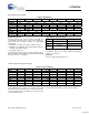
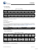
Timer n Register [R/W]
• Timer 0 Register 0xC010
• Timer 1 Register 0xC012
Figure 16. Timer n Register
Register Description
The Timer n Register sets the Timer n count. Both Timer 0 and Timer 1 decrement by one every 1-µs clock tick. Each can provide
an interrupt to the CPU when the timer reaches zero.
Count (Bits [15:0])
The Count field sets the Timer count.
General USB Registers
There is one set of registers dedicated to general USB control. This set consists of two identical registers, one for Host/Device
Port 1 and one for Host/Device Port 2. This register set has functions for both USB host and USB peripheral options and is covered
in this section and summarized in Table 22. USB Host-only registers are covered in Section “USB Host Only Registers” on page
19 and USB Device-only registers are covered in Section “USB Device Only Registers” on page 28.
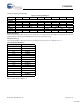
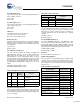
USB n Control Register [R/W]
• USB 1 Control Register 0xC08A
• USB 2 Control Register 0xC0AA
Figure 17. USB n Control Register
Register Description
The USB n Control register is used in both host and device mode. It monitors and controls the SIE and the data lines of the USB
ports. This register can be accessed by the HPI interface.
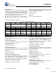
Bit # 15 14 13 12 11 10 9 8
Field Count...
Read/Write R/W R/W R/W R/W R/W R/W R/W R/W
Default 1 1 1 1 1 1 1 1
Bit # 7 6 5 4 3 2 1 0
Field ...Count
Read/Write R/W R/W R/W R/W R/W R/W R/W R/W
Default 1 1 1 1 1 1 1 1
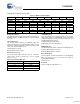
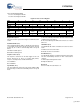
Table 22.USB Registers
Register Name Address (SIE1/SIE2) R/W
USB n Control Register 0xC08A/0xC0AA R/W
Bit # 15 14 13 12 11 10 9 8
Field
Reserved Port A
D+ Status
Port A
D– Status
Reserved LOA Mode
Select
Reserved
Read/Write - - R R - R/W R/W -
Default X X X X 0 0 0 0
Bit # 7 6 5 4 3 2 1 0
Field
Port A
Resistors Enable
Reserved Port A
Force D± State
Suspend
Enable
Reserved Port A
SOF/EOP Enable
Read/Write R/W - - R/W R/W R/W - R/W
Default 0 0 0 0 0 0 0 0
[+] Feedback