
User manual


CY7C67200
Document #: 38-08014 Rev. *G Page 39 of 78
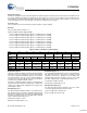
OTG Control Registers
There is one register dedicated for OTG operation. This
register is covered in this section and summarized in Ta ble 2 8.
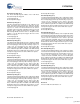
OTG Control Register [0xC098] [R/W]
Figure 40. OTG Control Register
Register Description
The OTG Control register allows control and monitoring over
the OTG port on Port1A.
VBUS Pull-up Enable (Bit 13)
The VBUS Pull-up Enable bit enables or disables a 500 ohm
pull-up resistor onto OTG VBus.
1: 500 ohm pull-up resistor enabled
0: 500 ohm pull-up resistor disabled
Receive Disable (Bit 12)
The Receive Disable bit enables or powers down (disables)
the OTG receiver section.
1: OTG receiver powered down and disabled
0: OTG receiver enabled
Charge Pump Enable (Bit 11)
The Charge Pump Enable bit enables or disables the OTG
VBus charge pump.
1: OTG VBus charge pump enabled
0: OTG VBus charge pump disabled
VBUS Discharge Enable (Bit 10)
The VBUS Discharge Enable bit enables or disables a 2K-ohm
discharge pull-down resistor onto OTG VBus.
1: 2K-ohm pull-down resistor enabled
0: 2K-ohm pull-down resistor disabled
D+ Pull-up Enable (Bit 9)
The D+ Pull-up Enable bit enables or disables a pull-up
resistor on the OTG D+ data line.
1: OTG D+ dataline pull-up resistor enabled
0: OTG D+ dataline pull-up resistor disabled
D– Pull-up Enable (Bit 8)
The D– Pull-up Enable bit enables or disables a pull-up
resistor on the OTG D– data line.
1: OTG D– dataline pull-up resistor enabled
0: OTG D– dataline pull-up resistor disabled
D+ Pull-down Enable (Bit 7)
The D+ Pull-down Enable bit enables or disables a pull-down
resistor on the OTG D+ data line.
1: OTG D+ dataline pull-down resistor enabled
0: OTG D+ dataline pull-down resistor disabled
D– Pull-down Enable (Bit 6)
The D– Pull-down Enable bit enables or disables a pull-down
resistor on the OTG D– data line.
1: OTG D– dataline pull-down resistor enabled
0: OTG D– dataline pull-down resistor disabled
OTG Data Status (Bit 2)
The OTG Data Status bit is a read only bit and indicates the
TTL logic state of the OTG VBus pin.
1: OTG VBus is greater than 2.4V
0: OTG VBus is less than 0.8V
ID Status (Bit 1)
The ID Status bit is a read only bit that indicates the state of
the OTG ID pin on Port A.
1: OTG ID Pin is not connected directly to ground (>10K ohm)
0: OTG ID Pin is connected directly ground (< 10 ohm)
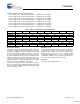
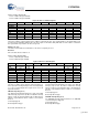
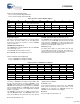
Table 28.OTG Registers
Register Name Address R/W
OTG Control Register C098H R/W
Bit # 15 14 13 12 11 10 9 8
Field Reserved VBUS
Pull-up
Enable
Receive
Disable
Charge Pump
Enable
VBUS
Discharge
Enable
D+
Pull-up
Enable
D–
Pull-up
Enable
Read/Write - - R/W R/W R/W R/W R/W R/W
Default 0 0 0 0 0 0 0 0
Bit # 7 6 5 4 3 2 1 0
Field D+
Pull-down
Enable
D–
Pull-down
Enable
Reserved OTG Data
Status
ID
Status
VBUS Valid
Flag
Read/Write R/W R/W - - - R R R
Default 0 0 0 0 0 X X X
[+] Feedback