
User manual

CY7C67200
Document #: 38-08014 Rev. *G Page 6 of 78
Charge Pump Features
• Meets OTG Supplement Requirements, see Table 41, “DC
Characteristics: Charge Pump,” on page 66.
Charge Pump Pins
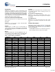
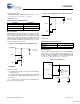
Booster Interface
EZ-OTG has an on-chip power booster circuit for use with
power supplies that range between 2.7V and 3.6V. The
booster circuit boosts the power to 3.3V nominal to supply
power for the entire chip. The booster circuit requires an
external inductor, diode, and capacitor. During power down
mode, the circuit is disabled to save power. Figure 2 shows
how to connect the booster circuit.
Component details:
• L1: Inductor with inductance of 10 µH and a current rating
of at least 250 mA
• D1: Schottky diode with a current rating of at least 250 mA
• C1: Tantalum or ceramic capacitor with a capacitance of at
least 2.2 µF
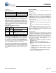
Figure 3 shows how to connect the power supply when the
booster circuit is not being used.
Booster Pins
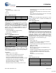
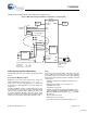
Crystal Interface
The recommended crystal circuit to be used with EZ-OTG is
shown in Figure 4. If an oscillator is used instead of a crystal
circuit, connect it to XTALIN and leave XTALOUT uncon-
nected. For further information on the crystal requirements,
see Table 39, “Crystal Requirements,” on page 65.
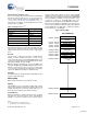
Table 11.Charge Pump Interface Pins
Pin Name Pin Number
OTGVBUS C1
CSwitchA D1
CSwitchB D2
Figure 2. Power Supply Connection With Booster
BOOSTVcc
VSWITCH
VCC
AVCC
C1
D1
L1
3.3V
2.7V to 3.6V
Power Supply
Figure 3. Power Supply Connection Without Booster
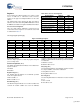
Table 12.Charge Pump Interface Pins
Pin Name Pin Number
BOOSTVcc F1
VSWITCH E2
Figure 4. Crystal Interface
BOOSTVcc
VSWITCH
VCC
AVCC
3.0V to 3.6V
Power Supply
Y1
C1 = 22 pF
C2 = 22 pF
CY7C67200
XTALIN
XTALOUT
12MHz
Parallel Resonant
Fundamental Mode
500uW
20-33pf ±5%
[+] Feedback