
User manual


CY7C67200
Document #: 38-08014 Rev. *G Page 65 of 78
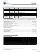
Absolute Maximum Ratings
This section lists the absolute maximum ratings. Stresses above those listed can cause permanent damage to the device.
Exposure to maximum rated conditions for extended periods can affect device operation and reliability.
Storage Temperature ............................................................................................................................................–40°C to +125°C
Ambient Temperature with Power Supplied............................................................................................................–40°C to +85°C
Supply Voltage to Ground Potential ...........................................................................................................................0.0V to +3.6V
DC Input Voltage to Any General Purpose Input Pin .............................................................................................................. 5.5V
DC Voltage Applied to XTALIN....................................................................................................................... –0.5V to V
CC
+ 0.5V
Static Discharge Voltage (per MIL-STD-883, Method 3015)............................................................................................. > 2000V
Max Output Current, per Input Output. .................................................................................................................................. 4 mA
Operating Conditions
T
A
(Ambient Temperature Under Bias)....................................................................................................................–40°C to +85°C
Supply Voltage (V
CC
, AV
CC
) ....................................................................................................................................+3.0V to +3.6V
Supply Voltage (BoostV
CC
)
[5]
...................................................................................................................................+2.7V to +3.6V
Ground Voltage........................................................................................................................................................................... 0V
F
OSC
(Oscillator or Crystal Frequency)............................................................................................................. 12 MHz ± 500 ppm
............................................................................................................................................................................ Parallel Resonant
Crystal Requirements (XTALIN, XTALOUT)
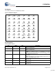
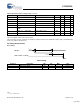
A6 Reserved – Tie to Gnd for normal operation.
F1 BOOSTV
CC
Power Booster Power Input: 2.7V to 3.6V
E2 VSWITCH Analog Output Booster Switching Output
E1 BOOSTGND Ground Booster Ground
C1 OTGVBUS Analog IO USB OTG Vbus
D1 CSWITCHA Analog Charge Pump Capacitor
D2 CSWITCHB Analog Charge Pump Capacitor
G1 AV
CC
Power USB Power
B1 AGND Ground USB Ground
H2, D6, A4 V
CC
Power Main V
CC
G6, B6, A1, H1 GND Ground Main Ground
Table 38.Pin Descriptions (continued)
Pin Name Type Description
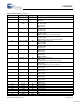
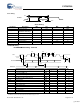
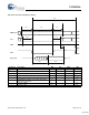
Table 39.Crystal Requirements
Crystal Requirements, (XTALIN, XTALOUT) Min. Typical Max. Unit
Parallel Resonant Frequency 12 MHz
Frequency Stability –500 +500 PPM
Load Capacitance 20 33 pF
Driver Level 500 µW
Start-up Time 5ms
Mode of Vibration: Fundamental
Note
5. The on-chip voltage booster circuit boosts BoostV
CC
to provide a nominal 3.3V V
CC
supply.
[+] Feedback