
User manual


CY7C67200
Document #: 38-08014 Rev. *G Page 73 of 78
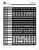
Register Summary
Table 42. Register Summary
R/W Address Register Bit 15 Bit 14 Bit 13 Bit 12 Bit 11 Bit 10 Bit 9 Bit 8 Default High
Bit 7 Bit 6 Bit 5 Bit 4 Bit 3 Bit 2 Bit 1 Bit 0 Default Low
R 0x0140 HPI Breakpoint Address... 0000 0000
...Address 0000 0000
R 0x0142 Interrupt Routing VBUS to HPI
Enable
ID to HPI
Enable
SOF/EOP2 to
HPI Enable
SOF/EOP2 to
CPU Enable
SOF/EOP1 to
HPI Enable
SOF/EOP1 to
CPU Enable
Reset2 to HPI
Enable
HPI Swap 1
Enable
0001 0100
Resume2 to
HPI Enable
Resume1 to
HPI Enable
Reserved Done2 to HPI
Enable
Done1 to HPI
Enable
Reset1 to HPI
Enable
HPI Swap 0
Enable
0000 0000
W 1: 0x0144
2: 0x0148
SIEXmsg Data... xxxx xxxx
...Data xxxx xxxx
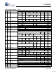
R/W 0x02n0 Device n Endpoint n Control Reserved xxxx xxxx
IN/OUT
Ignore Enable
Sequence
Select
Stall
Enable
ISO
Enable
NAK Interrupt
Enable
Direction
Select
Enable ARM
Enable
xxxx xxxx
R/W 0x02n2 Device n Endpoint n Address Address... xxxx xxxx
...Address xxxx xxxx
R.W 0x02n4 Device n Endpoint n Count Reserved Count... xxxx xxxx
...Count xxxx xxxx
R/W 0x02n6 Device n Endpoint n Status Reserved Overflow
Flag
Underflow
Flag
OUT
Exception Flag
IN
Exception Flag
xxxx xxxx
Stall
Flag
NAK
Flag
Length
Exception Flag
Set-up
Flag
Sequence
Status
Timeout
Flag
Error
Flag
ACK
Flag
xxxx xxxx
R/W 0x02n8 Device n Endpoint n Count Re-
sult
Result... xxxx xxxx
...Result xxxx xxxx
R 0xC000 CPU Flags Reserved... 0000 0000
...Reserved Global Inter-
rupt Enable
Negative
Flag
Overflow
Flag
Carry
Flag
Zero
Flag
000x xxxx
R/W 0xC002 Bank Address... 0000 0001
...Address Reserved 000x xxxx
R 0xC004 Hardware Revision Revision... xxxx xxxx
...Revision xxxx xxxx
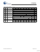
R/W 0xC006 GPIO Control Write Protect
Enable
UD Reserved SAS
Enable
Mode
Select
0000 0000
HSS
Enable
Reserved SPI
Enable
Reserved Interrupt 0
Polarity Select
Interrupt 0
Enable
0000 0000
R/W 0xC008 CPU Speed Reserved... 0000 0000
.Reserved CPU Speed 0000 000F
R/W 0xC00A Power Control Reserved Host/Device 2
Wake Enable
Reserved Host/Device 1
Wake Enable
OTG
Wake Enable
Reserved HSS
Wake Enable
SPI
Wake Enable
0000 0000
HPI
Wake Enable
Reserved GPI
Wake Enable
Reserved Boost 3V
OK
Sleep
Enable
Halt
Enable
0000 0000
R/W 0xC00C Watchdog Timer Reserved... 0000 0000
...Reserved Timeout
Flag
Period
Select
Lock
Enable
WDT
Enable
Reset
Strobe
0000 0000
R/W 0xC00E Interrupt Enable Reserved OTG
Interrupt
Enable
SPI
Interrupt
Enable
Reserved Host/Device 2
Interrupt
Enable
Host/Device 1
Interrupt
Enable
0000 0000
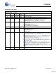
HSS Interrupt
Enable
In Mailbox
Interrupt
Enable
Out Mailbox
Interrupt
Enable
Reserved UART
Interrupt
Enable
GPIO
Interrupt
Enable
Timer 1
Interrupt
Enable
Timer 0
Interrupt
Enable
0001 0000
R/W 0xC098 OTG Control Reserved VBUS
Pull-up Enable
Receive
Disable
Charge Pump
Enable
VBUS Dis-
charge Enable
D+
Pull-up Enable
D–
Pull-up Enable
0000 0000
D+
Pull-down
Enable
D–
Pull-down
Enable
Reserved OTG Data Sta-
tus
ID
Status
VBUS Valid
Flag
0000 0XXX
R/W 0: 0xC010
1: 0xC012
Timer n Count... 1111 1111
...Count 1111 1111
R/W 0xC014 Breakpoint Address... 0000 0000
...Address 0000 0000
R/W 1: 0xC018
2: 0xC01A
Extended Page n Map Address...
...Address
R/W 0xC01E GPIO 0 Output Data GPIO15 GPIO14 GPIO13 GPIO12 GPIO11 GPIO10 GPIO9 GPIO8 0000 0000
GPIO7 GPIO6 GPIO5 GPIO4 GPIO3 GPIO2 GPIO1 GPIO0 0000 0000
R 0xC020 GPIO 0 Input Data GPIO15 GPIO14 GPIO13 GPIO12 GPIO11 GPIO10 GPIO9 GPIO8 0000 0000
GPIO7 GPIO6 GPIO5 GPIO4 GPIO3 GPIO2 GPIO1 GPIO0 0000 0000
R/W 0xC022 GPIO 0 Direction GPIO15 GPIO14 GPIO13 GPIO12 GPIO11 GPIO10 GPIO9 GPIO8 0000 0000
GPIO7 GPIO6 GPIO5 GPIO4 GPIO3 GPIO2 GPIO1 GPIO0 0000 0000
[+] Feedback