
User manual


CY7C67200
Document #: 38-08014 Rev. *G Page 9 of 78
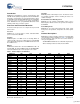
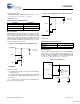
External (Remote) Wakeup Source
There are several possible events available to wake EZ-OTG
from Sleep mode as shown in Table 15. These may also be
used as remote wakeup options for USB applications. See
section “Power Control Register [0xC00A] [R/W]” on page 13.
Upon wakeup, code begins executing within 200 ms, the time
it takes the PLL to stabilize.
Power-On Reset (POR) Description
The length of the power-on-reset event can be defined by (V
CC
ramp to valid) + (Crystal start up). A typical application might
utilize a 12-ms power-on-reset event = ~7 ms + ~5 ms, respec-
tively.
Reset Pin
The Reset pin is active low and requires a minimum pulse
duration of sixteen 12-MHz clock cycles (1.3 ms). A reset
event restores all registers to their default POR settings. Code
execution then begins 200 ms later at 0xFF00 with an imme-
diate jump to 0xE000, the start of BIOS.
Note It should be noted that for up to 3 ms after BIOS starts
executing, GPIO[24:19] and GPIO[15:8] will be driven as out-
puts for a test mode. If these pins need to be used as inputs,
a series resistor is required (10 ohm to 48 ohm is recommend-
ed). Refer to BIOS documentation for addition details.
USB Reset
A USB Reset affects registers 0xC090 and 0xC0B0, all other
registers remain unchanged.
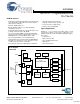
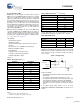
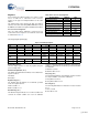
Memory Map
Memory map information is presented in this section.
Mapping
The EZ-OTG has just over 24 KB of addressable memory
mapped from 0x0000 to 0xFFFF. This 24 KB contains both
program and data space and is byte addressable. Figure 6.
shows the various memory region address locations.
Internal Memory
Of the internal memory, 15 KB is allocated for user’s program
and data code. The lower memory space from 0x0000 to
0x04A2 is reserved for interrupt vectors, general purpose
registers, USB control registers, the stack, and other BIOS
variables. The upper internal memory space contains EZ-OTG
control registers from 0xC000 to 0xC0FF and the BIOS ROM
itself from 0xE000 to 0xFFFF. For more information on the
reserved lower memory or the BIOS ROM, refer to the
Programmers documentation and the BIOS documentation.
During development with the EZ-OTG toolset, the lower area
of User's space (0x04A4 to 0x1000) should be left available to
load the GDB stub. The GDB stub is required to allow the
toolset debug access into EZ-OTG.
Figure 6. Memory Map
Table 15.wakeup Sources
[3, 4]
Wakeup Source (if enabled) Event
USB Resume D+/D– Signaling
OTGVBUS Level
OTGID Any Edge
HPI Read
HSS Read
SPI Read
IRQ0 (GPIO 24) Any Edge
Notes
3. Read data will be discarded (dummy data).
4. HPI_INT will assert on a USB Resume.registers
HW INTs
SW INTs
0x0000 - 0x00FF
Primary Registers
Swap Registers
USB Registers
HPI Int / Mailbox
Slave Setup Packet
BIOS
USER SPACE
~15K
Internal Memory
Control Registers
0x0100 - 0x011F
0x0120 - 0x013F
0x0140 - 0x0148
0x014A - 0x01FF
0x0200- 0x02FF
LCP Variables
0x0300- 0x030F
BIOS Stack0x0310- 0x03FF
USB Slave & OTG0x0400- 0x04A2
0x04A4- 0x3FFF
0xC000- 0xC0FF
0xE000- 0xFFFF
[+] Feedback