
User manual
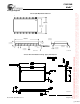

1-Mbit (128K x 8) Static RAM
CY62128B
MoBL
®
Cypress Semiconductor Corporation • 3901 North First Street • San Jose, CA 95134 • 408-943-2600
Document #: 38-05300 Rev. *C Revised March 7, 2005
Features
• Temperature Ranges
— Commercial: 0°C to 70°C
— Industrial: –40°C to 85°C
— Automotive: –40°C to 125°C
• 4.5V–5.5V operation
• CMOS for optimum speed/power
• Low active power
(70 ns, LL version, Commercial, Industrial)
— 82.5 mW (max.) (15 mA)
• Low standby power
(70 ns, LL version, Commercial, Industrial)
—110 µW (max.) (15 µA)
• Automatic power-down when deselected
• TTL-compatible inputs and outputs
• Easy memory expansion with CE
1
, CE
2
, and OE options
Functional Description
[1]
The CY62128B is a high-performance CMOS static RAM
organized as 131,072 words by 8 bits. Easy memory
expansion is provided by an active LOW Chip Enable (CE
1
),
an active HIGH Chip Enable (CE
2
), an active LOW Output
Enable (OE
), and three-state drivers. This device has an
automatic power-down feature that reduces power
consumption by more than 75% when deselected.
Writing to the device is accomplished by taking Chip Enable
One (CE
1
) and Write Enable (WE) inputs LOW and Chip
Enable Two (CE
2
) input HIGH. Data on the eight I/O pins (I/O
0
through I/O
7
) is then written into the location specified on the
address pins (A
0
through A
16
).
Reading from the device is accomplished by taking Chip
Enable One (CE
1
) and Output Enable (OE) LOW while forcing
Write Enable (WE
) and Chip Enable Two (CE
2
) HIGH. Under
these conditions, the contents of the memory location
specified by the address pins will appear on the I/O pins.
The eight input/output pins (I/O
0
through I/O
7
) are placed in a
high-impedance state when the device is deselected (CE
1
HIGH or CE
2
LOW), the outputs are disabled (OE HIGH), or
during a write operation (CE
1
LOW, CE
2
HIGH, and WE LOW).
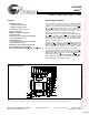
The CY62128B is available in a standard 450-mil-wide SOIC,
32-pin TSOP type I and STSOP packages.
Note:
1. For best-practice recommendations, please refer to the Cypress application note “System Design Guidelines” on http://www.cypress.com.
14
15
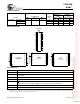
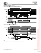
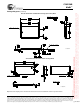
Logic Block Diagram
A
1
A
2
A
3
A
4
A
5
A
6
A
7
A
8
COLUMN
DECODER
ROW DECODER
SENSE AMPS
INPUT BUFFER
POWER
DOWN
WE
OE
I/O
0
CE
2
I/O
1
I/O
2
I/O
3
512x256x8
ARRAY
I/O
7
I/O
6
I/O
5
I/O
4
A
0
A
11
A
13
A
12
A
A
10
CE
1
A
A
16
A
9
[+] Feedback