
nvSRAM With Real Time Clock Specification Sheet

CY14B101K
Document Number: 001-06401 Rev. *I Page 6 of 28
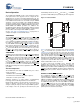
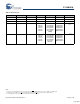
Table 2. Mode Selection
CE WE OE
A15 – A0 Mode IO Power
H X X X Not Selected Output High Z Standby
L H L X READ SRAM Output Data Active
L L X X WRITE SRAM Input Data Active
L H L 0x4E38
0xB1C7
0x83E0
0x7C1F
0x703F
0x8FC0
Read SRAM
Read SRAM
Read SRAM
Read SRAM
Read SRAM
Nonvolatile
STORE
Output Data
Output Data
Output Data
Output Data
Output Data
Output High Z
Active I
CC2
[1, 2, 3]
L H L 0x4E38
0xB1C7
0x83E0
0x7C1F
0x703F
0x4C63
Read SRAM
Read SRAM
Read SRAM
Read SRAM
Read SRAM
Nonvolatile
RECALL
Output Data
Output Data
Output Data
Output Data
Output Data
Output High Z
Active
[1, 2, 3]
Notes
1. The six consecutive address locations are in the order listed. WE
is HIGH during all six cycles to enable a nonvolatile cycle.
2. While there are 17 address lines on the CY14B101K, only the lower 16 lines are used to control software modes.
3. O state depends on the state of OE
. The IO table shown is based on OE Low.
[+] Feedback