
1 Mbit nvSRAM Specification Sheet

CY14B101L
Document Number: 001-06400 Rev. *I Page 4 of 18
Hardware RECALL (Power Up)
During power up or after any low power condition (V
CC
<
V
SWITCH
), an internal RECALL request is latched. When V
CC
once again exceeds the sense voltage of V
SWITCH
, a RECALL
cycle is automatically initiated and takes t
HRECALL
to complete.
Software STORE
Data is transferred from the SRAM to the nonvolatile memory by
a software address sequence. The CY14B101L software
STORE cycle is initiated by executing sequential CE controlled
READ cycles from six specific address locations in exact order.
During the STORE cycle, an erase of the previous nonvolatile
data is first performed followed by a program of the nonvolatile
elements. When a STORE cycle is initiated, input and output are
disabled until the cycle is completed.
Because a sequence of READs from specific addresses is used
for STORE initiation, it is important that no other READ or WRITE
accesses intervene in the sequence. If they intervene, the
sequence is aborted and no STORE or RECALL takes place.
To initiate the software STORE cycle, the following READ
sequence is performed:
1. Read address 0x4E38, Valid READ
2. Read address 0xB1C7, Valid READ
3. Read address 0x83E0, Valid READ
4. Read address 0x7C1F, Valid READ
5. Read address 0x703F, Valid READ
6. Read address 0x8FC0, Initiate STORE cycle
The software sequence is clocked with CE
controlled READs or
OE
controlled READs. When the sixth address in the sequence
is entered, the STORE cycle commences and the chip is
disabled. It is important that READ cycles and not WRITE cycles
are used in the sequence. It is not necessary that OE
is LOW for
a valid sequence. After the t
STORE
cycle time is fulfilled, the
SRAM is again activated for READ and WRITE operation.
Software RECALL
Data is transferred from the nonvolatile memory to the SRAM by
a software address sequence. A software RECALL cycle is
initiated with a sequence of READ operations in a manner similar
to the software STORE initiation. To initiate the RECALL cycle,
the following sequence of CE
controlled READ operations is
performed:
1. Read address 0x4E38, Valid READ
2. Read address 0xB1C7, Valid READ
3. Read address 0x83E0, Valid READ
4. Read address 0x7C1F, Valid READ
5. Read address 0x703F, Valid READ
6. Read address 0x4C63, Initiate RECALL cycle
Internally, RECALL is a two step procedure. First, the SRAM data
is cleared, and then the nonvolatile information is transferred into
the SRAM cells. After the t
RECALL
cycle time, the SRAM is once
again ready for READ and WRITE operations. The RECALL
operation does not alter the data in the nonvolatile elements. The
nonvolatile data can be recalled an unlimited number of times.
Data Protection
The CY14B101L protects data from corruption during low
voltage conditions by inhibiting all externally initiated STORE
and WRITE operations. The low voltage condition is detected
when V
CC
is less than V
SWITCH
.
If the CY14B101L is in a WRITE mode (both CE
and WE are low)
at power up after a RECALL or after a STORE, the WRITE is
inhibited until a negative transition on CE
or WE is detected. This
protects against inadvertent writes during power up or brown out
conditions.
Noise Considerations
The CY14B101L is a high speed memory. It must have a high
frequency bypass capacitor of approximately 0.1 µF connected
between V
CC
and V
SS,
using leads and traces that are as short
as possible. As with all high speed CMOS ICs, careful routing of
power, ground, and signals reduce circuit noise.
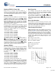
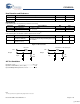
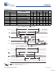
Low Average Active Power
CMOS technology provides the CY14B101L the benefit of
drawing significantly less current when it is cycled at times longer
than 50 ns. Figure 3 shows the relationship between I
CC
and
READ or WRITE cycle time. Worst case current consumption is
shown for both CMOS and TTL input levels (commercial temper-
ature range, VCC = 3.6V, 100% duty cycle on chip enable). Only
standby current is drawn when the chip is disabled. The overall
average current drawn by the CY14B101L depends on the
following items:
■
The duty cycle of chip enable
■
The overall cycle rate for accesses
■
The ratio of READs to WRITEs
■
CMOS versus TTL input levels
■
The operating temperature
■
The V
CC
level
■
IO loading
Figure 3. Current Versus Cycle Time
[+] Feedback