
nvSRAM Specification Sheet


PRELIMINARY
CY14B101LA, CY14B101NA
Document #: 001-42879 Rev. *B Page 14 of 25
Hardware STORE Cycle
Parameters Description
20ns 25ns 45ns
Unit
Min Max Min Max Min Max
t
DHSB
HSB To Output Active Time when write latch not set 20 25 25 ns
t
PHSB
Hardware STORE Pulse Width 15 15 15 ns
t
SS
[29, 30]
Soft Sequence Processing Time 100 100 100 μs
Switching Waveforms
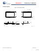
Figure 14. Hardware STORE Cycle
[23]
Figure 15. Soft Sequence Processing
[29, 30]
t
PHSB
t
PHSB
t
DELAY
t
DHSB
t
DELAY
t
STORE
t
HHHD
t
LZHSB
Write latch set
Write latch not set
HSB (IN)
HSB (OUT)
DQ (Data Out)
RWI
HSB (IN)
HSB (OUT)
RWI
HSB pin is driven high to V
CC
only by Internal
SRAM is disabled as long as HSB (IN) is driven low.
HSB driver is disabled
t
DHSB
100kOhm resistor,
Address #1 Address #6 Address #1 Address #6
Soft Sequence
Command
t
SS
t
SS
CE
Address
V
CC
t
SA
t
CW
Soft Sequence
Command
t
CW
Notes
29. This is the amount of time it takes to take action on a soft sequence command. Vcc power must remain HIGH to effectively register command.
30. Commands such as STORE and RECALL lock out IO until operation is complete which further increases this time. See the specific command.
[+] Feedback