
Specifications


STK17TA8
Document #: 001-52039 Rev. *C Page 12 of 24
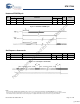
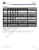
MODE Selection
E W G A
16
-A
0
Mode I/O Power Notes
H X X X Not Selected Output High Z Standby
L H L X Read SRAM Output Data Active
L L X X Write SRAM Input Data Active
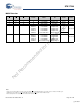
L H L 0x04E38
0x0B1C7
0x083E0
0x07C1F
0x0703F
Read SRAM
Read SRAM
Read SRAM
Read SRAM
Read SRAM
Output Data
Output Data
Output Data
Output Data
Output Data
Active 18, 19, 20
0x08FC0 Nonvolatile Store Output High Z I
CC2
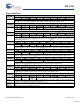
L H L 0x04E38
0x0B1C7
0x083E0
0x07C1F
0x0703F
0x04C63
Read SRAM
Read SRAM
Read SRAM
Read SRAM
Read SRAM
Nonvolatile Recall
Output Data
Output Data
Output Data
Output Data
Output Data
Output High Z
Active
18, 19, 20
Notes
18. The six consecutive addresses must be in the order listed. W
must be high during all six consecutive cycles to enable a nonvolatile cycle.
19. While there are 17 addresses on the STK17TA8, only the lower 16 are used to control software modes
20. I/O state depends on the state of G
. The I/O table shown assumes G low
[+] Feedback
Not Recommended for New Designs