
Specifications


STK17TA8
Document #: 001-52039 Rev. *C Page 13 of 24
nvSRAM Operation
The STK17TA8 nvSRAM is made up of two functional compo-
nents paired in the same physical cell. These are the SRAM
memory cell and a nonvolatile QuantumTrap cell. The SRAM
memory cell operates like a standard fast static RAM. Data in the
SRAM can be transferred to the nonvolatile cell (the STORE
operation), or from the nonvolatile cell to SRAM (the RECALL
operation). This unique architecture enables all cells to be stored
and recalled in parallel. During the STORE and RECALL opera-
tions SRAM READ and WRITE operations are inhibited. The
STK17TA8 supports unlimited read and writes like a typical
SRAM. In addition, it provides unlimited RECALL operations
from the nonvolatile cells and up to 200K STORE operations.
SRAM READ
The STK17TA8 performs a READ cycle whenever E and G are
low while W
and HSB are high. The address specified on pins
A
0-16
determine which of the 131,072 data bytes are accessed.
When the READ is initiated by an address transition, the outputs
are valid after a delay of t
AVQV
(READ cycle #1). If the READ is
initiated by E
and G, the outputs are valid at t
ELQV
or at t
GLQV
,
whichever is later (READ cycle #2). The data outputs repeatedly
respond to address changes within the t
AVQV
access time
without the need for transitions on any control input pins, and
remain valid until another address change or until E
or G is
brought high, or W
and HSB is brought low.
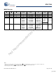
Figure 14. AutoStore Mode
SRAM WRITE
A WRITE cycle is performed whenever E and W are low and HSB
is high. The address inputs must be stable prior to entering the
WRITE cycle and must remain stable until either E
or W goes
high at the end of the cycle. The data on the common I/O pins
DQ0-7 is written into memory if it is valid t
DVWH
before the end
of a W
controlled WRITE or t
DVEH
before the end of an E
controlled WRITE.
It is recommended that G
be kept high during the entire WRITE
cycle to avoid data bus contention on common I/O lines. If G
is
left low, internal circuitry turns off the output buffers t
WLQZ
after
W
goes low.
AutoStore Operation
The STK17TA8 stores data to nvSRAM using one of three
storage operations. These three operations are Hardware Store
(activated by HSB
), Software Store (activated by an address
sequence), and AutoStore (on power down).
AutoStore operation, a unique feature of Cypress QuantumTrap
technology is a standard feature on the STK17TA8.
During normal operation, the device draws current from V
CC
to
charge a capacitor connected to the V
CAP
pin. This stored
charge is used by the chip to perform a single STORE operation.
If the voltage on the V
CC
pin drops below V
SWITCH
, the part
automatically disconnects the V
CAP
pin from V
CC
. A STORE
operation is initiated with power provided by the V
CAP
capacitor.
Figure 14 shows the proper connection of the storage capacitor
(V
CAP
) for automatic store operation. Refer to the DC Electrical
Characteristics on page 4 for the size of the capacitor. The
voltage on the V
CAP
pin is driven to 5V by a charge pump internal
to the chip. A pull up should be placed on W
to hold it inactive
during power up.
To reduce unneeded nonvolatile stores, AutoStore and
Hardware Store operations are ignored unless at least one
WRITE operation has taken place since the most recent STORE
or RECALL cycle. Software initiated STORE cycles are
performed regardless of whether a WRITE operation has taken
place. The HSB signal can be monitored by the system to detect
an AutoStore cycle is in progress.
Hardware STORE (HSB) Operation
The STK17TA8 provides the HSB pin for controlling and
acknowledging the STORE operations. The HSB
pin can be
used to request a hardware STORE cycle. When the HSB
pin is
driven low, the STK17TA8 conditionally initiates a STORE
operation after t
DELAY
. An actual STORE cycle only begins if a
WRITE to the SRAM took place since the last STORE or
RECALL cycle. The HSB pin has a very resistive pullup and is
internally driven low to indicate a busy condition while the
STORE (initiated by any means) is in progress. This pin should
be externally pulled up if it is used to drive other inputs.
SRAM READ and WRITE operations that are in progress when
HSB
is driven low by any means are given time to complete
before the STORE operation is initiated. After HSB
goes low, the
STK17TA8 continues to allow SRAM operations for t
DELAY
.
During t
DELAY
, multiple SRAM READ operations may take place.
If a WRITE is in progress when HSB
is pulled low, it is allowed a
time, t
DELAY
, to complete. However, any SRAM WRITE cycles
requested after HSB
goes low is inhibited until HSB returns high.
If HSB
is not used, it should be left unconnected.
Hardware RECALL (POWER UP)
During power up or after any low power condition
(V
CC
<V
SWITCH
), an internal RECALL request is latched. When
V
CC
once again exceeds the sense voltage of V
SWITCH
, a
RECALL cycle is automatically initiated and takes t
HRECALL
to
complete.
Software STORE
Data can be transferred from the SRAM to the nonvolatile
memory by a software address sequence. The STK17TA8
software STORE cycle is initiated by executing sequential E
controlled or G controlled READ cycles from six specific address
locations in exact order. During the STORE cycle, previous data
is erased and then the new data is programmed into the nonvol-
V
CC
V
CAP
10k Ohm
0.1µF
V
CC
V
CAP
W
[+] Feedback
Not Recommended for New Designs