
Specifications


STK17TA8
Document #: 001-52039 Rev. *C Page 20 of 24
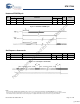
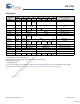
0x1FFF7
Watchdog Timer
D7 D6 D5 D4 D3 D2 D1 D0
WDS WDW WDT
WDS Watchdog Strobe. Setting this bit to 1 reloads and restarts the watchdog timer. The bit is cleared automatically
once the watchdog timer is reset. The WDS bit is write only. Reading it always will return a 0.
WDW Watchdog Write Enable. Set this bit to 1 to disable writing of the watchdog time-out value (WDT5-WDT0). This
allows the user to strobe the watchdog stobe bit without disturbing the time-out value. Set this bit to 0 to allow bits
5-0 to be written.
WDT Watchdog time-out selection. The watchdog timer interval is selected by the 6-bit value in this register. It represents
a multiplier of the 32 Hz count (31.25 ms). The range of time-out values is 31.25 ms (a setting of 1) to 2 seconds
(setting of 3Fh). Setting the watchdog timer register to 0 disables the timer. These bits can be written only if the
WDW bit was cleared to 0 on a previous cycle.
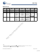
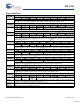
0x1FFF6
Interrupt
D7 D6 D5 D4 D3 D2 D1 D0
WIE AIE PFIE ABE H/L P/L 0 0
WIE Watchdog Interrupt Enable. When set to 1 and a watchdog time-out occurs, the watchdog timer drives the INT pin
as well as setting the WDF flag. When set to 0, the watchdog time-out only sets the WDF flag.
AIE Alarm Interrupt Enable. When set to 1, the alarm match drives the INT pin as well as setting the AF flag. When set
to 0, the alarm match only affects the AF flag.
PFIE Power-Fail Enable. When set to 1, a power failure drives the INT pin as well as setting the PF flag. When set to 0,
the power failure only sets the PF flag.
0 Reserved For Future Used
H/L High/Low. When set to a 1, the INT pin is driven active high. When set to 0, the INT pin is open drain, active low.
P/L Pulse/Level. When set to a 1, the INT pin is driven active (determined by H/L) by an interrupt source for approxi-
mately 200 ms. When set to a 0, the INT pin is driven to an active level (as set by H/L) until the Flags register is read.
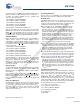
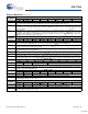
0x1FFF5
Alarm – Day
D7 D6 D5 D4 D3 D2 D1 D0
M 0 10s Alarm Date Alarm Date
Contains the alarm value for the date of the month and the mask bit to select or deselect the date value.
M Match. Setting this bit to 0 causes the date value to be used in the alarm match. Setting this bit to 1 causes the
match circuit to ignore the date value.
0x1FFF4
Alarm – Hours
D7 D6 D5 D4 D3 D2 D1 D0
M 0 10s Alarm Hours Alarm Hours
Contains the alarm value for the hours and the mask bit to select or deselect the hours value.
M Match. Setting this bit to 0 causes the hours value to be used in the alarm match. Setting this bit to 1 causes the
match circuit to ignore the hours value.
Register Map Detail (continued)
[+] Feedback
Not Recommended for New Designs