
nvSRAM Specification Sheet

PRELIMINARY
CY14B101LA, CY14B101NA
Document #: 001-42879 Rev. *B Page 8 of 25
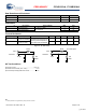
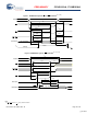
AC Test Conditions
Input Pulse Levels.................................................... 0V to 3V
Input Rise and Fall Times (10% - 90%)........................ <
3 ns
Input and Output Timing Reference Levels.................... 1.5V
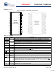
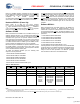
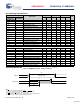
Data Retention and Endurance
Parameter Description Min Unit
DATA
R
Data Retention 20 Years
NV
C
Nonvolatile STORE Operations 200 K
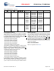
Capacitance
Parameter
[14]
Description Test Conditions Max Unit
C
IN
Input Capacitance T
A
= 25°C, f = 1 MHz,
V
CC
= 0 to 3.0V
7pF
C
OUT
Output Capacitance 7 pF
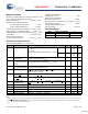
Thermal Resistance
Parameter
[14]
Description Test Conditions 48-FBGA 48-SSOP 44-TSOP II 32-SOIC Unit
Θ
JA
Thermal Resistance
(Junction to Ambient)
Test conditions follow standard
test methods and procedures for
measuring thermal impedance,
in accordance with EIA/JESD51.
28.82 TBD 31.11 TBD °C/W
Θ
JC
Thermal Resistance
(Junction to Case)
7.84 TBD 5.56 TBD °C/W
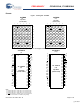
Figure 5. AC Test Loads
3.0V
OUTPUT
5 pF
R1
R2
789Ω
3.0V
OUTPUT
30 pF
R1
R2
789Ω
for tri-state specs
577Ω
577Ω
Note
14. These parameters are guaranteed by design and are not tested.
[+] Feedback