
Serial SPI nvSRAM Specification Sheet

PRELIMINARY
CY14B101P
Document #: 001-44109 Rev. *B Page 6 of 32
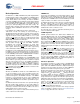
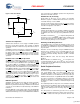
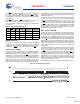
SPI Modes
CY14B101P device may be driven by a microcontroller with its
SPI peripheral running in either of the following two modes:
■
SPI Mode 0 (CPOL=0, CPHA=0)
■
SPI Mode 3 (CPOL=1, CPHA=1)
For both these modes, input data is latched in on the rising edge
of Serial Clock (SCK) starting from the first rising edge after CS
goes active. If the clock starts from a HIGH state (in mode 3), the
first rising edge after the clock toggles are considered. The
output data is available on the falling edge of Serial Clock (SCK).
The two SPI modes are shown in Figure 4 and Figure 5. The
status of clock when the bus master is in Standby mode and not
transferring data is:
■
SCK remains at 0 for Mode 0
■
SCK remains at 1 for Mode 3
CPOL and CPHA bits must be set in the SPI controller for the
either Mode 0 or Mode 3. CY14B101P detects the SPI mode
from the status of SCK pin when device is selected by bringing
the CS
pin LOW. If SCK pin is LOW when device is selected, SPI
Mode 0 is assumed and if SCK pin is HIGH, CY14B101P works
in SPI Mode 3.
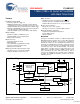
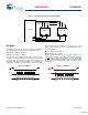
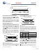
Figure 3. System Configuration Using SPI nvSRAM
P101B41YCP101B41YC
uController
SCK
MOSI
MISO
SI SO OSISKCSSCK
CS
HOLD HOLDCS
CS1
CS2
HOLD1
HOLD2
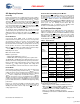
Figure 4. SPI Mode 0
LSB
MSB
765432
10
CS
SCK
SI
0 1 2 3 4 5 6 7
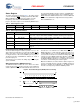
Figure 5. SPI Mode 3
CS
SCK
SI
765432
10
LSB
MSB
0 12 34 56 7
[+] Feedback