
1 Mbit nvSRAM Specification Sheet

PRELIMINARY
1 Mbit (128K x 8) Serial SPI nvSRAM
CY14B101Q1
CY14B101Q2
CY14B101Q3
Cypress Semiconductor Corporation • 198 Champion Court • San Jose, CA 95134-1709 • 408-943-2600
Document #: 001-50091 Rev. *A Revised February 2, 2009
Features
■ 1 Mbit NonVolatile SRAM
❐ Internally organized as 128K x 8
❐ STORE to QuantumTrap
®
nonvolatile elements initiated au-
tomatically on power down (AutoStore
®
) or by user using
HSB pin (Hardware Store) or SPI instruction (Software Store)
❐ RECALL to SRAM initiated on power up (Power Up Recall
®
)
or by SPI Instruction (Software RECALL)
❐ Automatic STORE on power down with a small capacitor
■ High Reliability
❐ Infinite Read, Write, and RECALLl cycles
❐ 200,000 STORE cycles to QuantumTrap
❐ Data Retention: 20 Years
■ High Speed Serial Peripheral Interface (SPI)
❐ 40 MHz Clock rate
❐ Supports SPI Modes 0 (0,0) and 3 (1,1)
■ Write Protection
❐ Hardware Protection using Write Protect (WP) Pin
❐ Software Protection using Write Disable Instruction
❐ Software Block Protection for 1/4,1/2, or entire Array
■ Low Power Consumption
❐ Single 3V +20%, –10% operation
❐ Average Vcc current of 10 mA at 40 MHz operation
■ Industry Standard Configurations
❐ Commercial and industrial temperatures
❐ CY14B101Q1 has identical pin configuration to industry stan-
dard 8-pin NV Memory
❐ 8-pin DFN and 16-pin SOIC Packages
❐ RoHS compliant
Functional Overview
The Cypress CY14B101Q1/CY14B101Q2/CY14B101Q3
combines a 1 Mbit nonvolatile static RAM with a nonvolatile
element in each memory cell. The memory is organized as 128K
words of 8 bits each. The embedded nonvolatile elements incor-
porate the QuantumTrap technology, creating the world’s most
reliable nonvolatile memory. The SRAM provides infinite read
and write cycles, while the QuantumTrap cell provides highly
reliable nonvolatile storage of data. Data transfers from SRAM to
the nonvolatile elements (STORE operation) takes place
automatically at power down. On power up, data is restored to
the SRAM from the nonvolatile memory (RECALL operation).
Both STORE and RECALL operations can also be triggered by
the user.
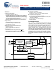
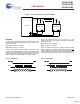
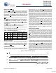
Instruction
register
Address
Decoder
Data I/O register
Status register
Power Control
STORE/RECALL
Control
Instruction decode
Write protect
Control logic
Quantum Trap
STORE
RECALL
SI
SCK
V
CC
V
CAP
SO
HSB
128K X 8
SRAM ARRAY
128K X 8
A0-A16
D0-D7
HOLD
CS
WP
Logic Block Diagram
[+] Feedback